Difference between revisions of "Velleman PCSU1000"
Jump to navigation
Jump to search
(Created page with 'The [http://www.velleman.eu/products/view/?id=362986 Velleman PCSU1000] is an inexpensive USB-based oscilloscope. It has 2 channels, an analog bandwidth of 50MHz and 1GS/s sampli…') |
Uwe Hermann (talk | contribs) m |
||
| Line 5: | Line 5: | ||
== Components == | == Components == | ||
TODO | * Xilinx XC3S50 | ||
* Microchip PIC16F630-I/P | |||
* FTDI FT245BL | |||
* 50MHz crystal: 50.000 Y0KE | |||
* Microchip 93LC46BI | |||
* Philips/NXP 74HC367D | |||
* SIR-S4-105A FZ | |||
* Unisonic Technologies Co. (UTC) ULN2003 | |||
TODO: Rest of the chips. | |||
== Photos == | |||
<gallery> | |||
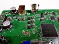
File:Velleman pcsu1000 pcb front.jpg|<small>PCB, front</small> | |||
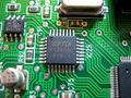
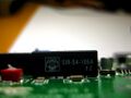
File:Velleman pcsu1000 pcb chunk.jpg|<small>PCB, chunk</small> | |||
File:Velleman pcsu1000 xilinx xc3s50.jpg|<small>Xilinx XC3S50</small> | |||
File:Velleman pcsu1000 microchip pic16f630 ip.jpg|<small>Microchip PIC16F630-I/P</small> | |||
File:Velleman pcsu1000 ftdi ft245bl.jpg|<small>FTDI FT245BL</small> | |||
File:Velleman pcsu1000 microchip 93lc46bi.jpg|<small>Microchip 93LC46BI</small> | |||
File:Velleman pcsu1000 uln2003.jpg|<small>UTC ULN2003</small> | |||
File:Velleman pcsu1000 nxp 74hc367d.jpg|<small>Philips/NXP 74HC367D</small> | |||
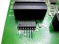
File:Velleman pcsu1000 3x soic8.jpg|<small>3x SOIC-8 chips</small> | |||
File:Velleman pcsu1000 50mhz crystal.jpg|<small>50MHZ crystal</small> | |||
File:Velleman pcsu1000 sir s4 105a fz.jpg|<small>SIR-S4-105A FZ</small> | |||
</gallery> | |||
Photo TODO: Device front, device back, connectors, PCB back, unreadable chip on the "PCB chunk" photo, others. | |||
== Protocol == | == Protocol == | ||
TODO | TODO | ||
Revision as of 20:06, 29 April 2012
The Velleman PCSU1000 is an inexpensive USB-based oscilloscope. It has 2 channels, an analog bandwidth of 50MHz and 1GS/s sampling rate.
See Velleman PCSU1000/Info for more details (such as lsusb -vvv output) about the device.
Components
- Xilinx XC3S50
- Microchip PIC16F630-I/P
- FTDI FT245BL
- 50MHz crystal: 50.000 Y0KE
- Microchip 93LC46BI
- Philips/NXP 74HC367D
- SIR-S4-105A FZ
- Unisonic Technologies Co. (UTC) ULN2003
TODO: Rest of the chips.
Photos
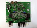
PCB, front
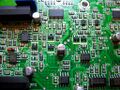
PCB, chunk
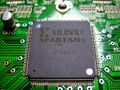
Xilinx XC3S50
Microchip PIC16F630-I/P
FTDI FT245BL
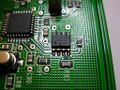
Microchip 93LC46BI
UTC ULN2003
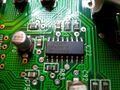
Philips/NXP 74HC367D
3x SOIC-8 chips
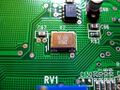
50MHZ crystal
SIR-S4-105A FZ


Photo TODO: Device front, device back, connectors, PCB back, unreadable chip on the "PCB chunk" photo, others.
Protocol
TODO