Difference between revisions of "Fx2grok"
Uwe Hermann (talk | contribs) (→Schematics, PCB layout, 3D preview: fx2grok-tiny 0.2 schematics, layout, 3D preview) |
Uwe Hermann (talk | contribs) (→Assembly: fx2grok-tiny 0.2 photos) |
||
| Line 212: | Line 212: | ||
<gallery> | <gallery> | ||
File:Fx2grok 0 | File:Fx2grok 0 2 pcb panel.jpg|<small>PCB panel</small> | ||
File:Fx2grok 0 | File:Fx2grok 0 2 pcbs.jpg|<small>PCBs</small> | ||
File:Fx2grok 0 | File:Fx2grok 0 2 pcb top.jpg|<small>PCB, top</small> | ||
File:Fx2grok 0 | File:Fx2grok 0 2 pcb bottom.jpg|<small>PCB, bottom</small> | ||
File:Fx2grok 0 | File:Fx2grok 0 2 stencil top.jpg|<small>Stencil, top</small> | ||
File:Fx2grok 0 2 stencil bottom.jpg|<small>Stencil, bottom</small> | |||
File:Fx2grok 0 | File:Fx2grok 0 2 solderpaste.jpg|<small>Solderpaste</small> | ||
File:Fx2grok 0 | File:Fx2grok 0 2 pcb top populated.jpg|<small>PCB, top, populated</small> | ||
File:Fx2grok 0 | File:Fx2grok 0 2 pcb bottom populated.jpg|<small>PCB, bottom, populated</small> | ||
File:Fx2grok 0 | File:Fx2grok 0 2 device top.jpg|<small>Device, top</small> | ||
File:Fx2grok 0 2 device bottom.jpg|<small>Device, bottom</small> | |||
File:Fx2grok 0 | File:Fx2grok 0 2 device and cable.jpg|<small>Device and cable</small> | ||
File:Fx2grok 0 | File:Fx2grok 0 2 size comparison.jpg|<small>Size comparison</small> | ||
File:Fx2grok 0 | |||
File:Fx2grok 0 | |||
</gallery> | </gallery> | ||
Revision as of 14:26, 16 December 2017
The fx2grok family consists of four devices (fx2grok-flat, fx2grok-tiny, fx2grok-bga, fx2grok-wide) of very small, Open Hardware FX2-based logic analyzers.
The schematics and layouts are done from scratch in KiCad, and are released under the CC-BY-SA 4.0 license.
Using the open-source fx2lafw firmware (and sigrok, of course) you can use these devices as 8-channel (or 16-channel, for the fx2grok-wide) logic analyzers.
Device comparison
Note: All of this is work in progress and might change at any time!
| Item | fx2grok-flat | fx2grok-tiny | fx2grok-bga | fxgrok-wide |
|---|---|---|---|---|
| Goals 2 |
|
|
|
|
| Author | Piotr Esden-Tempski | Uwe Hermann | Uwe Hermann | Ryan "Izzy" Bales, based off of Piotr Esden-Tempski's fx2grok-flat |
| Hardware license | CC-BY-SA 4.0 | CC-BY-SA 4.0 1 | CC-BY-SA 4.0 | CC-BY-SA 4.0 |
| Size | 33 mm x 16 mm | 11 mm x 11 mm | tbd | tbd |
| Logic channels | 8 + CLK & TRIG | 8 | tbd | 16 |
| Layout specs |
|
|
tbd | tbd |
| Cypress FX2 | Cypress CY7C68013A-56LTXC, QFN, 8 mm x 8 mm | Cypress CY7C68013A-56LTXC, QFN, 8 mm x 8 mm | Cypress CY7C68013A-56BAXC, BGA, 5 mm x 5 mm | Cypress CY7C68013A-56LTXC, QFN, 8 mm x 8 mm |
| Input protection | 3 x IP425x-4-TTL EMI/ESD filters on all probes + 100k pull-ups, 1x USBLC6-2 for USB | None whatsoever | None whatsoever | 100Ω on each probe, 4x DSILC6-4 for all probes, 1x USBLC6-2 for USB |
| 24 MHz crytal | ABM8 | 4-SMD, 300μW, 2 mm x 1.6 mm | tbd | tbd |
| USB connector | USB Micro-B SMD | USB Micro-B SMD | tbd | USB Micro-B SMD |
| Probe connector | 2x6 1.27 mm PCB-edge connector | 2x5 1.27 mm PCB-edge connector | tbd | 2x 2x5 1.27 mm PCB-edge connectors |
| EEPROM | Yes, sigrok fx2lafw (8-channel) VID/PID 1d50:608c | None, default Cypress VID/PID 04b4:8613 | None, default Cypress VID/PID 04b4:8613 | Yes, sigrok fx2lafw (16-channel) VIP/PID 1d50:608d |
| Passives | Mostly 0402, some 0603 & 0.4 mm pitch DFN | Only 0402 | tbd | Mostly 0402, some 0603 |
| LED | 1x 0603 LED on PA1 | 1x 0402 LED on PA1 | tbd | 1x 0603 LED on PA1 |
1 The obsolete/nonworking fx2grok-tiny 0.1 was licensed CC-BY-SA 3.0, since version 0.2 the license is CC-BY-SA 4.0.
2 Optional goal: Make a tiny 3D-printed enclosure, and/or an "enclosure" using resin (example) with the device (including probes) ideally looking similar to the sigrok logo in the end.
What is NOT the goal?
As you may know, there are tons of FX2-based logic analyzers (and tons of clones) already. There's not much use in creating yet another "standard" device.
The goal of this little hobby project is thus NOT to make a better device, or to make a cheaper device, or anything like that. The only goal is to have it as tiny as possible (it's more of a "just for fun" project).
Status
fx2grok-tiny 0.2 has been tested and is known to work. The first PCB version (fx2grok-tiny 0.1) is not working and thus obsolete.
Download
The schematics, PCB layout and Gerber files are available from the fx2grok Git repository:
$ git clone git://sigrok.org/fx2grok
Photos
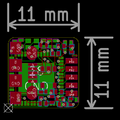
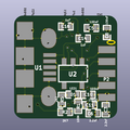
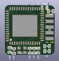
Schematics, PCB layout, 3D preview
fx2grok-tiny 0.2:
fx2grok-flat 0.2:
Cable and connector variants
Samtec SFSD-05-28-H-10.00-SR + TFM-105-01-L-D:
Hand-soldered ribbon cable:
Assembly
Bill of materials
fx2grok-tiny 0.2
Note: All prices are for single quantities, most parts get a lot cheaper if you buy higher quantities.
| Qty | Device | Footprint | Size | Value | Refdes | Digikey | Mouser | Comments |
|---|---|---|---|---|---|---|---|---|
| Required parts | ||||||||
| 1 | Cypress CY7C68013A-56LTXC | QFN-56 | 8 mm x 8 mm | — | IC1 | 10.05€ | 10.30€ | Main chip. Alternatives:
|
| 1 | Amphenol FCI 10118192-0001LF | custom | 9.8 mm x 5.6 mm | — | U1 | 0.38€ | 0.35€ | USB Micro-B SMD connector |
| 1 | Murata XRCGB24M000FAN00R0 | custom | 2 mm x 1.6 mm | 24 MHz | Y1 | 0.29€ | 0.46€ | 24MHz crystal, ±25ppm, 6pF, 150 Ohms, max. 300μW drive level, 4-SMD, no lead |
| 1 | Micrel MIC5504-3.3YM5-TR | SOT-23-5 | 2.9 mm x 1.6 mm | 3.3 V | U2 | 0.10€ | 0.10€ | 3.3 V LDO, max. 300mA |
| 4 | Yageo RC0402JR-072R7L | 0402 | 0.25 mm x 0.125 mm | 2.7 kΩ | R2, R3, R4, R5 | 0.08€ | 0.08€ | Resistor |
| 1 | Samsung RC1005J104CS | 0402 | 0.25 mm x 0.125 mm | 100 kΩ | R1 | 0.08€ | — | Resistor |
| 8 | Samsung CL05A104KP5NNNC | 0402 | 0.25 mm x 0.125 mm | 100 nF | C2, C5, C7, C8, C10-C13 | 0.08€ | — | Ceramic capacitor |
| 3 | Taiyo Yuden JMK105BJ105KV-F | 0402 | 0.25 mm x 0.125 mm | 1 µF | C1, C14, C16 | 0.08€ | 0.10€ | Ceramic capacitor |
| 2 | Murata GRM155R61A225KE95D | 0402 | 0.25 mm x 0.125 mm | 2.2 µF | C3, C6 | 0.08€ | 0.08€ | Ceramic capacitor |
| 2 | Samsung CL05C120JB5NNNC | 0402 | 0.25 mm x 0.125 mm | 12 pF | C4, C9 | 0.08 | — | Ceramic capacitor |
| 1 | Vishay VLMB1500-GS08 | 0402 | 0.25 mm x 0.125 mm | — | D1 | 0.34€ | 0.51€ | LED |
| Optional parts / variants | ||||||||
| 1 | Amphenol FCI 20021111-00010T4LF | custom | — | — | P1/P2 | 0.53€ | 0.55€ | 5x2 through-hole pin header (1.27 mm pitch), could soldered to the PCB (5 pins per side) |
| 1 | Amphenol FCI 20021311-00010T4LF | custom | — | — | — | 0.68€ | 0.69€ | 5x2 connector/receptacle (1.27 mm pitch), could be used for soldering the probe cable/wires |
| 1 | Samtec TFM-105-01-L-D | custom | — | — | P1/P2 | 0.53€ | — | 5x2 through-hole pin header (1.27 mm pitch) with a notch, soldered to the PCB (5 pins per side), match for the Samtec SFSD-05-28-H-10.00-SR cable below |
| 1 | Samtec SFSD-05-28-H-10.00-SR | custom | — | — | — | 4.77€ | — | Potential probe cable, needs some crimping |
Note: C15 is missing and there is a C16, which is correct. C15 was removed and the numbering wasn't reset.
Resources
- Cypress FX2 overview page
- CY7C68013A, CY7C68014A, CY7C68015A, CY7C68016A datasheet (PDF)
- EZ-USB Technical Reference Manual (TRM) (PDF)
- AN15456 - Guide to a Successful EZ-USB FX2LP Hardware Design (PDF)
- esden's series of videos on the fx2grok-flat design (schematics, PCB, with background information and almost a KiCad tutorial)
- esden's GitHub repository with the KiCad project files for the fx2grok-flat (in the "flat" branch)
- Ryan's GitHub repository with the KiCad project files for the fx2grok-wide (in the "wide" branch)


