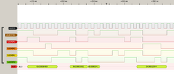
Protocol decoder:aud
 | |
| Name | AUD |
|---|---|
| Description | Renesas/Hitachi Advanced User Debugger (AUD) protocol |
| Status | supported |
| License | GPLv2+ |
| Source code | decoders/aud |
| Input | logic |
| Output | aud |
| Probes | AUDCK, nAUDSYNC, AUDATA3-AUDATA0 |
| Optional probes | — |
| Options | — |
Renesas/Hitachi AUD (Advanced User Debugger)
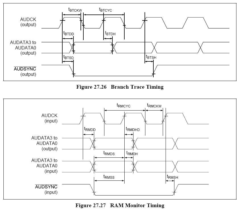
The AUD (Advanced User Debugger) port of certain Renesas / Hitachi microcontrollers has two modes of peration, "Branch Trace mode" and "RAM monitor mode".
Currently the protocol decoder implementation only recognizes "Branch Trace" mode.
The AUD protocol is described in the microcontroller datasheets, such as rej09b0046 - SH7058 Hardware manual
Refer to the AUD chapter for functional description, and the AC characteristics chapter for timing diagrams.
Interface description
The interface itself is 4 data lines, and 4 control lines (reset, clock, mode, sync):
- AUDCK
- nAUDSYNC
- nAUDRST
- nAUDMD
- AUDATA3
- AUDATA2
- AUDATA1
- AUDATA0
Modes of operation
Branch trace mode
In this mode, the mcu generates the clock signal on AUDCK (typically 20MHz) and shifts out a 4-bit nibble every clock. The value reconstructed from those nibbles is the destination address of any jump, branch, or call instruction changing the PC register. Specialized or very fast hardware is required to read the data. FPGA / CPLD based interfaces, or a logic analyzer capable of sampling at least 6 simultaneous channels at >= 80MSps, can do this. 40MSps gives very inconsistent results since the sampling clock is certainly at least a few ppm away from the target clock, and the AUDCK edges are sometimes missed.
Alternately, a logic analyzer capable of state analysis at 20MHz (capturing on rising edges of AUDCK) should be sufficient. Unfortunately, cheap hardware like Logic/Logic16 clones do not support this.
RAM monitor mode
The AUD port accepts commands to read/write to the RAM. Decoding this mode is not implemented at the moment.
