Difference between revisions of "Protocol decoder:Spiflash"
Uwe Hermann (talk | contribs) m |
Uwe Hermann (talk | contribs) m |
||
| Line 1: | Line 1: | ||
{{DISPLAYTITLE:mx25lxx05d}} | {{DISPLAYTITLE:Protocol decoder:mx25lxx05d}} | ||
<div style="float:right"> | <div style="float:right"> | ||
{{Infobox protocol decoder | {{Infobox protocol decoder | ||
Revision as of 00:03, 26 November 2012
 | |
| Name | Macronix MX25Lxx05D |
|---|---|
| Description | SPI-attached serial EEPROM |
| Status | supported |
| License | GPLv2+ |
| Source code | decoders/mx25lxx05d |
| Input | spi, logic |
| Output | mx25lxx05d |
| Probes | — |
| Optional probes | HOLD#, WP#/ACC |
| Options | — |
The mx25lxx05d protocol decoder supports the Macronix MX25L1605D / MX25L3205D / MX25L6405D SPI (NOR) flash chip protocol.
Hardware
Chip pinout
The Macronix MX25Lxx05D chips have the following pinout:
| CS# | 1- | O | -8 | VCC |
| SO | 2- | -7 | HOLD# | |
| WP# | 3- | -6 | SCLK | |
| GND | 4- | -5 | SI |
Macronix MX25L1605D in openbiosprog-spi
The spi/mx25l1605d directory in sigrok-dumps contains a set of example captures of a Macronix MX25L1605D (MX25L1605DPI-12G) SPI flash chip (16Mbit == 2Mbyte; NOR flash) that is probed, being written to, read, or erased.
The logic analyzer used was a ChronoVu LA8 (at 25MHz). It is probing the SPI chip in the openbiosprog-spi Open Hardware USB-based SPI chip programmer. The host software used is flashrom.
Probe setup:
| Probe | MX25L1605D pin |
|---|---|
| 0 (green) | CS# |
| 1 (orange) | SO/SIO1 (a.k.a MISO) |
| 2 (white) | SCLK |
| 3 (red) | SI/SIO0 (a.k.a MOSI) |
| 4 (gray) | WP#/ACC |
| 5 (brown) | HOLD# |
Photos:
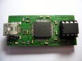
openbiosprog-spi with chip
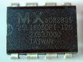
Macronix MX25L1605D
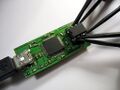
Chip, probed


Protocol
The chip uses the standard SPI protocol and pins (MISO, MOSI, SCLK, CS#), with the additional (optional) HOLD# and WP#/ACC pins.
The host can send a large number of commands to the SPI chip (such as WREN, RDID, READ, SE, CE, PP, and many more). The commands have various length, and usually consist of one command ID byte, optional address bytes, one or more data/payload bytes, and so on (depending on the command).
TODO: Detailed protocol description.