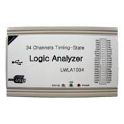
Sysclk LWLA1034
Jump to navigation
Jump to search
 | |
| Status | supported |
|---|---|
| Source code | sysclk-lwla |
| Channels | 34 |
| Samplerate | 125MHz (max) |
| Samplerate (state) | ? |
| Triggers | 34 + extern |
| Min/max voltage | 0-5V |
| Threshold voltage | ? |
| Memory | 256Kbit/channel |
| Compression | RLE |
| Website | aliexpress.com |
The Sysclk LWLA1034 is a USB-based, 34-channel logic analyzer with up to 125MHz sampling rate.
See Sysclk LWLA1034/Info for more details (such as lsusb -v output) about the device.
Hardware
- Altera EP2C5Q208C8N (Cyclone II) FPGA
- Cypress CY7C68013A-56 (FX2) USB interface chip
- Cypress 256k×36 SRAM (likely a CY7C1361C-133AXC or similar)
- STC15F104E 8051-based microcontroller
The not-installed 10-pin connector between the USB socket and the large capacitor seems to connect to the JTAG pins of the FPGA.
Photos
(Note: The yellow/greenish markings weren't there, they're added by the photographer)
PCB for another device:
Software
Firmware
We have received permission from the vendor to distribute the FPGA bitstreams with sigrok. Thus, the bitstreams are now included in the sigrok-firmware module.
- The FX2 firmware is loaded from an EEPROM on the board, so that the final USB device descriptor is immediately available on power-up.
- Endpoint 4 is used exclusively for loading a new bitstream into the FPGA.
- Endpoint 2 is used for sending commands to the FPGA firmware, with responses (if any) coming in from endpoint 6.
Reverse engineering of the vendor's custom protocol has been completed. See Sysclk LWLA1034/Protocol for the documentation.


