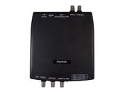
Hantek DDS-3X25
Jump to navigation
Jump to search
 | |
| Status | planned |
|---|---|
| Frequency (user) | 25MHz |
| Waveforms | user only |
| Waveform memory | 4000 points |
| Amplitude | 0 - 3.5V |
| Connectivity | USB |
| Website | hantek.com |
The Hantek DDS-3X25 is a 25MHz PC-based function generator. It has no external controls, requiring a USB connection to a computer.
See Hantek DDS-3X25/Info for more details (such as lsusb -vvv output) about the device.
Hardware
- FPGA: Xylinx Spartan? 144 pins (20 MHz clock)
- Microcontroller: STM32F103C6(T6A) Mainstream Performance line, ARM Cortex-M3 MCU with 32 Kbytes Flash, 72 MHz CPU, motor control, USB and CAN (8 MHz? clock)
- Output amplifier: LMH6702 1.7 GHz, Ultra Low Distortion, Wideband Op Amp.
- Sync signal output is connected without any buffer or amplifier.
- COUNT IN is connected through TL3016 ULTRA-FAST LOW-POWER PRECISION COMPARATOR.
- Isolated unregulated DC-DC converter MORNSUN A0505S-2W, ±5V, ±200mA
Photos
Protocol
Waveform samples
When sending a waveform to the device, a series of samples denote voltage. These are 12-bit values packed in padded 16-bit integers, sent in network order (most significant part first):
- bits 0-9 are the value, with encoding as shown below
- bit 10
- bit 11 is the sign: 1 for positive, 0 for negative
- bit 12 controls the "sync out" port: 1 is on, 0 is off
- bits 13 is always 1, bits 14-15 are always 0
The value is encoded as 2048 - (voltage * 585). Negative values have all sign and value bits complemented (reversed).
0xA0: configure
Configures the device. The payload is 6 bytes:
| Byte | Bit | Description |
|---|---|---|
| 1 | Mode | |
| 7 | ||
| 6 | ||
| 5 | 1 = Reset external trigger (send only once) | |
| 4 | 1 = External trigger mode enabled | |
| 3 | External trigger: 0 = falling, 1 = rising | |
| 2 | 0 = continuous, 1 = single wave | |
| 1 | Counter reset: 0 = leave, 1 = reset | |
| 0 | Measurement: 0 = frequency, 1 = counter | |
| 2 | ||
| 7 | ||
| 6 | ||
| 5 | ||
| 4 | ||
| 3 | ||
| 2 | ||
| 1 | ||
| 0 | Output: 0 = pattern generator, 1 = programmable output | |
| 3 | Digital I/O pins, bits 0-7 | |
| 4 | Bits 0-3 = digital I/O pins bits 8-11, bits 4-7 unused | |
| 5 | Clock divider, based on 48KHz clock | |
| 6 |
THe response is 10 bytes:
- the first 2 bytes are always 0
- in frequency measurement mode:
- four bytes for the current frequency measurement, in network order. Multiply by 2 to get the actual frequency readout.
- four bytes for a "tick counter" in network order. This has the number of ticks per second, and is used to derive the frequency. Assuming a 100Mhz clock, this counter differs up to 4.17% at 8Mhz from the derived frequency -- investigate.
- in counter mode:
- four bytes for the current counter, in network order.
- four bytes denoting the smoothed out frequency, identical to the first four bytes in frequency measurement mode.
0xA1: point transfer indicator
The payload is 2 bytes:
| Byte | Bit | Description |
|---|---|---|
| 1 | 0-7 | Bits 0-7 of the waveform point count |
| 2 | 0-3 | Bits 8-11 of the waveform point count |
| 4-6 | Unused | |
| 7 | 0=transfer end, 1=transfer start |
There is a 1-byte response: 0xcc
0xA2: unknown
- 6-byte payload: 0000 0000 3000
- 1-byte response: 0xcd
When setting "close output power on", i.e. save configuration to memory:
- no payload
- 1-byte response: 0xcd
0xA3: unknown
- no payload
- 1-byte response: 0x02


