Difference between revisions of "Protocol decoder:Avr pdi"
Uwe Hermann (talk | contribs) |
(AVR PDI, minor formatting nits for screenshots) |
||
| Line 38: | Line 38: | ||
== Screenshots == | == Screenshots == | ||
''' | '''Screenshots from using the GUI''' | ||
<gallery widths=800px> | |||
<gallery> | |||
File:pd-pdi-annotate-zoom.png|<small>Detailled annotation in zoom levels</small> | File:pd-pdi-annotate-zoom.png|<small>Detailled annotation in zoom levels</small> | ||
File:pd-pdi-enable-pdibus.png|<small>Enable PDIBUS mmap access</small> | File:pd-pdi-enable-pdibus.png|<small>Enable PDIBUS mmap access</small> | ||
| Line 49: | Line 47: | ||
</gallery> | </gallery> | ||
Command line use, textual output | '''Command line use, binary and textual output''' | ||
<small> | <small> | ||
Latest revision as of 22:28, 26 December 2016
 | |
| Name | AVR PDI |
|---|---|
| Description | Atmel Program and Debug Interface |
| Status | supported |
| License | GPLv2+ |
| Source code | decoders/avr_pdi |
| Input | logic |
| Output | avr_pdi |
| Probes | reset, data |
| Optional probes | — |
| Options | — |
The avr_pdi protocol decoder can decode Atmel's proprietary Program and Debug Interface protocol which is used to program (write and read internal flash and other types of memory) and debug (control execution of software) Atmel ATxmega MCUs.
Hardware
The PDI protocol involves two mandatory signals: The RESET pin is used as PDI_CLK, another dedicated pin is named PDI_DATA. Typical clock rate is in the range of few hundred kHz to several MHz.
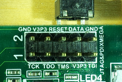
The Xplain eval board contains a 10pin programming header which carries both the JTAG and the PDI signals (see the info box in the upper right hand corner).
Atmel suggests universal use of a 6pin header (1 DATA, 2 VCC, 5 CLK, 6 GND) such that standard cables can be used with their programmers, and no adaption is required between the differing pinouts.
Protocol
The physical layer is UART-like but clocked (synchronous). The clock is provided by the programmer. Data gets sampled at the rising clock edge (both TX and RX). Communication is bidirectional and half-duplex, the device only sends response data upon the programmer's request.
A frame consists of a start bit, eight data bits (LSB first), an even parity bit, and a number of stop bits.
The UART layer communicates byte values. The first byte contains an instruction opcode, and optionally size/length specs for its operands. The set of operands depends on the respective opcode. Subsequent bytes carry the instruction's operands, and/or memory content which gets written or retrieved by running a sequence of intrinsic PDI operations.
By accessing the device's internal memory space, and the register set of internal peripherals (especially the NVM controller), the programmer can identify the target, and read and write several kinds of memory in the device (flash, EEPROM, fuses, signatures).
Access to memory is publicly documented, the protocol for debugging might not be (I'd be glad to be wrong on this).
Screenshots
Screenshots from using the GUI
Command line use, binary and textual output
 $ sigrok-cli -i identify.sr -P avr_pdi -B avr_pdi=bytes | hexdump -Cv
 00000000  c2 03 82 03 c0 fd 80 00  c1 59 e0 ff 88 d8 cd 45  |.........Y.....E|
 00000010  ab 89 12 80 02 80 02 0c  ca 01 00 01 00 0c c4 01  |................|
 00000020  00 01 f9 6b 90 00 00 01  a1 02 00 24 1e 97 4c 4c  |...k.......$..LL|
 00000030  ca 01 00 01 00 4c c4 01  00 01 f9 c1 00 c0 00 80  |.....L..........|
 00000040  00                                                |.|
 $ sigrok-cli -i identify.sr -P avr_pdi -A avr_pdi=cmd-data
 STCS ctrl 0x03
 LDCS ctrl 0x03
 STCS status 0xfd
 LDCS status 0x00
 STCS reset 0x59
 KEY 0x1289ab45cdd888ff
 LDCS status 0x02
 LDCS status 0x02
 LDS 0x010001ca 0x00
 LDS 0x010001c4 0xf9
 ST ptr 0x01000090
 REPEAT 0x0002
 LD *(ptr++) 0x1e 0x97 0x4c
 STS 0x010001ca 0x00
 STS 0x010001c4 0xf9
 STCS reset 0x00
 STCS status 0x00
 LDCS status 0x00


