Difference between revisions of "Hameg HMO2524"
m (HMO2524 is supported, SCPI link) |
(mechanical PCB arrangement, notes on boards' chips) |
||
| (One intermediate revision by the same user not shown) | |||
| Line 19: | Line 19: | ||
See [[Hameg HO730]] for the Ethernet/USB communication module (optional extra). | See [[Hameg HO730]] for the Ethernet/USB communication module (optional extra). | ||
( | Hardware construction: The handle can get removed at one of the eight possible angles, A "tube style" metal can then slides towards the back. | ||
There is a digital board at the left hand side, in a vertical orientation, plugged into one of the analog boards. | |||
There are two analog boards at the bottom of the device, connected to each other with pin headers. | |||
One analog board has shielded input sections for the analog channels and holds the rear connectors. | |||
Another analog board holds the digital pods and has huge analog chips and heat sinks. | |||
At the top there is the power supply and the communication interface. The fan at the rear is silent. | |||
Analog board 1: | |||
* four shielded input sections | |||
* Altera MAX-II CPLD | |||
* some TI chip near external connectors | |||
Analog board 2: | |||
* three locations for BGA chips, two of them populated | |||
* probably two DAC chips for two analog channels each | |||
* four DRAM chips, two on each PCB side | |||
Digital board: | |||
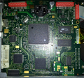
* Hitachi SH3 SoC (center position, other chips clockwise) | |||
* SST flash 39V.. | |||
* Elpida DRAM | |||
* NatSemi chip (display driver?) | |||
* Altera Cyclone-II FPGA (hardware support for protocol decoding) | |||
* ISSI RAM (for Cypress chip) | |||
* Cypress USB connectivity | |||
* TI chip for DVI display | |||
* connectors (clockwise, from top left): comm interface, power supply, front keyboard / encoders (?), front display, 2x17 test points (??), analog board connection, DVI, USB host | |||
== Photos == | == Photos == | ||
| Line 27: | Line 53: | ||
File:hmo2524-back.png|<small>back view</small> | File:hmo2524-back.png|<small>back view</small> | ||
File:hz350-total.png|<small>HZ350 probe</small> | File:hz350-total.png|<small>HZ350 probe</small> | ||
File:hmo2524-teardown-top-comm-psu.png|<small>teardown, top view, comm interface, power supply</small> | |||
File:hmo2524-teardown-bottom-analog-1.png|<small>teardown, bottom view, analog boards</small> | |||
File:hmo2524-teardown-bottom-analog-2.png|<small>teardown, bottom view, analog board, zoom</small> | |||
File:hmo2524-teardown-bottom-analog-3.png|<small>teardown, bottom view, analog boards connection</small> | |||
File:hmo2524-teardown-inside-analog-1.png|<small>teardown, inside view, analog boards</small> | |||
File:hmo2524-teardown-inside-analog-2.png|<small>teardown, inside view, analog boards</small> | |||
File:hmo2524-teardown-inside-analog-3.png|<small>teardown, inside view, analog chips, bird's view</small> | |||
File:hmo2524-teardown-side-digital-1.png|<small>teardown, side view, digital board</small> | |||
File:hmo2524-teardown-side-digital-2.png|<small>teardown, side view, digital board</small> | |||
</gallery> | </gallery> | ||
Latest revision as of 17:29, 11 February 2017
The Hameg HMO2524 is a 4-channel oscilloscope with an analog bandwidth of 250MHz and 2.5GS/s sampling rate. Two of the four channels optionally can get used as digital ports with 8 lines each. Communication is done via USB/RS232 (standard option), or Ethernet or IEEE-488 (extra options).
Although the HMO2524 model number starts with 2, it has features that only are found in models of the HMO3000 family. Which is why HMO2524 seems to be somewhere "in between" the Hameg HMO compact series and HMO3000. In the meantime the HMO2524 model "has vanished" from the vendor's site. That's independent from the R&S acquisition.
Hardware
The HMO2524 shipped with four HZ350 analog probes. See Hameg HO3508 for the digital probes (optional extra). The front has connectors for analog and digital probes, signals for calibration, and USB host (for flash drives).
The back has connectors for mains power, communication (interfaces are optional), USB host, DVI (only 640x480 regardless of monitor size), Y-OUT and external trigger. See Hameg HO720 for the USB/RS232 communication module (comes with the device by default). See Hameg HO730 for the Ethernet/USB communication module (optional extra).
Hardware construction: The handle can get removed at one of the eight possible angles, A "tube style" metal can then slides towards the back. There is a digital board at the left hand side, in a vertical orientation, plugged into one of the analog boards. There are two analog boards at the bottom of the device, connected to each other with pin headers. One analog board has shielded input sections for the analog channels and holds the rear connectors. Another analog board holds the digital pods and has huge analog chips and heat sinks. At the top there is the power supply and the communication interface. The fan at the rear is silent.
Analog board 1:
- four shielded input sections
- Altera MAX-II CPLD
- some TI chip near external connectors
Analog board 2:
- three locations for BGA chips, two of them populated
- probably two DAC chips for two analog channels each
- four DRAM chips, two on each PCB side
Digital board:
- Hitachi SH3 SoC (center position, other chips clockwise)
- SST flash 39V..
- Elpida DRAM
- NatSemi chip (display driver?)
- Altera Cyclone-II FPGA (hardware support for protocol decoding)
- ISSI RAM (for Cypress chip)
- Cypress USB connectivity
- TI chip for DVI display
- connectors (clockwise, from top left): comm interface, power supply, front keyboard / encoders (?), front display, 2x17 test points (??), analog board connection, DVI, USB host
Photos
Protocol
The Hameg HMO series of scopes use SCPI as the communication protocol.


