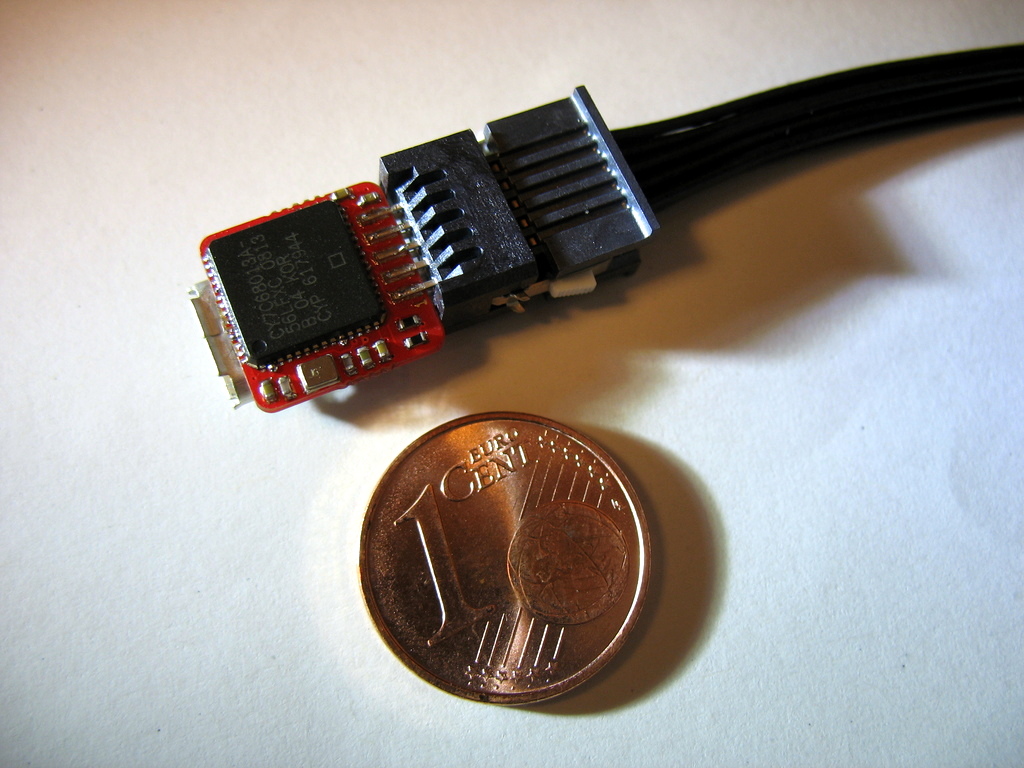
 This blog post won't be about the sigrok software for a change. Instead, it is meant to introduce a little hobby project for a tiny DIY FX2 based Open Hardware logic analyzer (that you can use with sigrok, of course): fx2grok-tiny.
The original plan for a tiny logic analyzer was devised by me (Uwe Hermann) in 2012, but being a sigrok developer, I've concentrated on various more important tasks, features, and bugs in the sigrok stack for quite a while. Near the end of 2017 I finally got around to finishing this project.
So the plan was to make an 8-channel, 24MHz FX2 based logic analyzer that is
* Open Hardware (CC-BY-SA 4.0 license for schematics and layout),
* uses Open Source EDA tools (KiCad),
* uses Open Source software on the PC side (libsigrok, PulseView),
* uses Open Source firmware on the FX2 microcontroller (sigrok-firmware-fx2lafw),
* and is as tiny as possible
 As you probably know, there are tons of (larger) FX2 based LAs around already, so there's no point to make just yet another one of those. What's unique about this one is that it's completely open, and it may just be the smallest logic analyzer on the planet (don't quote me on that, though).
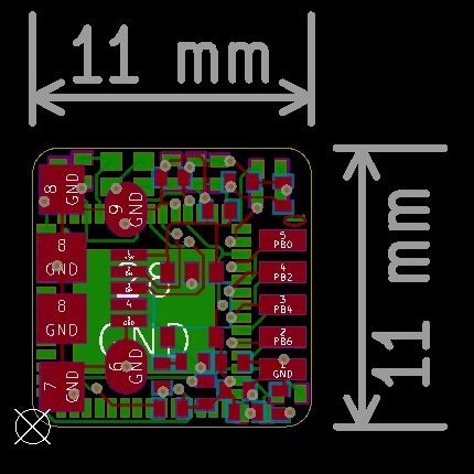
The original plan was to fit all required components in a 13x13mm PCB, but the final device ended up being even a little smaller, 11x11mm. The limiting factors are the Cypress CY7C68013A (a.k.a. FX2) chip itself (QFN-56, 8x8mm) plus the micro USB connector and 24MHz crystal, so getting it even smaller than 11x11mm is not easily possible.
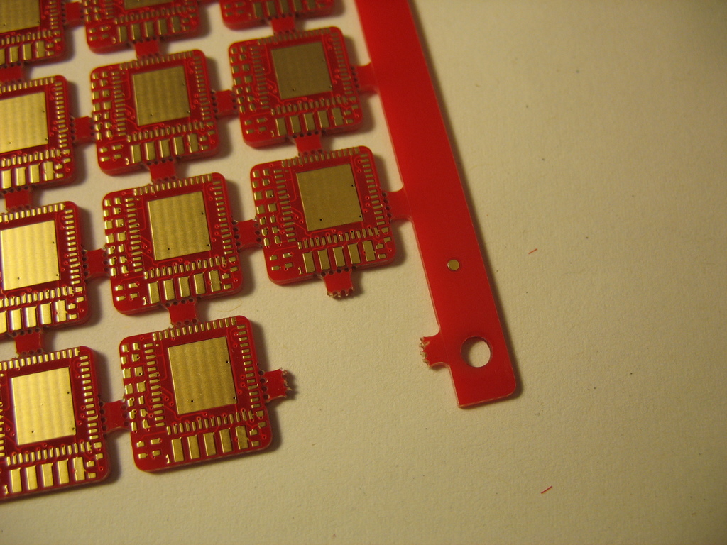 I'm using a 2-layer PCB (components on both sides), 5 mil traces, 6 mil trace clearance, 8 mil via drill hole diameter, 5 mil annular ring. The PCB has to be 0.8mm thick so that the 5x2 1.27mm PCB edge connector will fit. All passives are 0402.
The design intentionally sacrifices a lot of things (no EEPROM, no input protection, various Cypress hardware recommendations are ignored) in order to be able to make it very tiny.
This project was a lot of fun for me. Being a software guy, I learned quite a bit about creating schematics and doing PCB layouts (in KiCad), PCB manufacturing details, solder stencil and solder oven usage, and lots more. I also learned that when you screw up the FX2 footprint, you'll get magic smoke (that's why the final version is 0.2, I had to completely reroute the whole PCB after fixing the footprint).
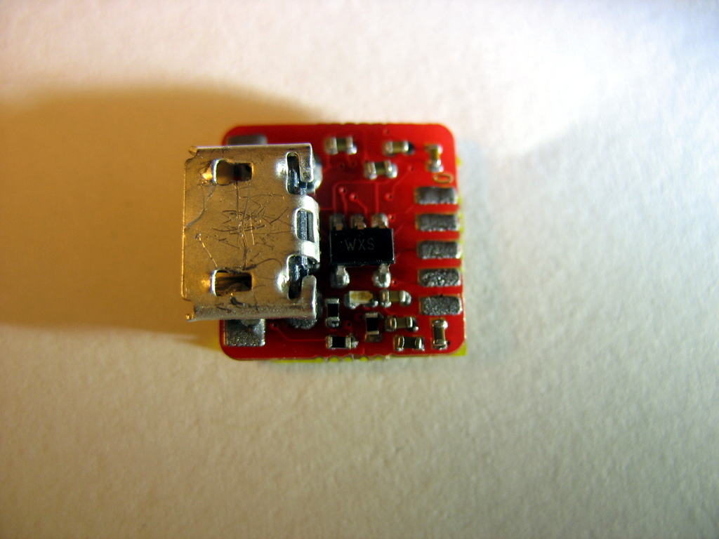
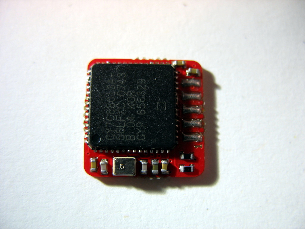 If you're wondering whether you can order fx2grok-tiny devices or bare PCBs, the answer is no. This is a purely non-commercial hobby project by a single guy. You can, however, make your own devices since everything is open and documented.
As an "enclosure" of sorts you can simply use e.g. transparent heatshrink tube. I'm also working on a tiny 3D printable enclosure, we'll see how that goes.
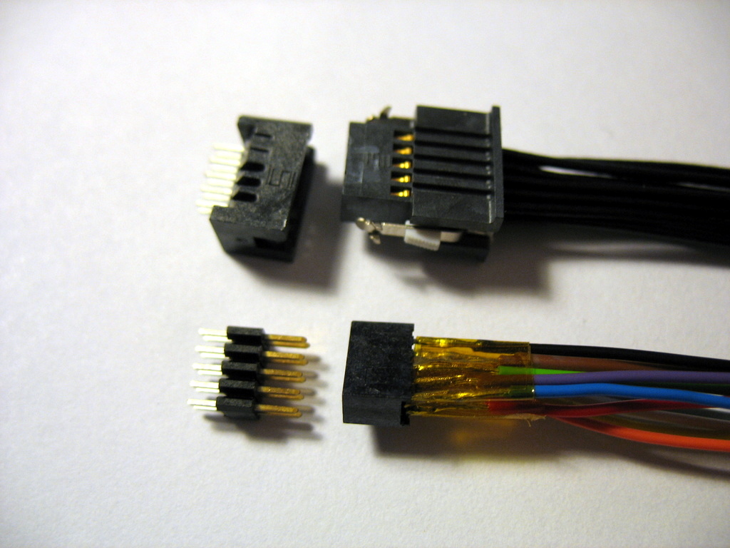 As for the probe cables there are various options as well. You can use a nice Samtec cable or just solder a DIY cable out of generic ribbon cable. In both cases, you'll have to use a crimp tool so you can later attach the usual logic analyzer grippers.
The fx2grok wiki page has a lot more details and photos about the device (including a BOM, you can get pretty much all required parts from e.g. Digikey) and how to assemble it.
You can also get the whole KiCad project, schematics, layout, and Gerber files via git:
$ git clone git://sigrok.org/fx2grok
 There's also a blue LED on the PCB for the obligatory blinkenlights, btw. It'll blink during a logic analyzer acquisition and just light up constantly in idle.
For the future I'm looking into maybe creating an even smaller FX2 based logic analyzer named fx2grok-bga, which employs (you guessed it) the BGA version of the FX2. The BGA chip is 5x5mm (instead of 8x8mm for the QFN version). Soldering this is going to be a bit more tricky though, we'll see how it goes.
There are also other fx2grok variants being worked on, e.g. fx2grok-flat by Piotr Esden-Tempski, more about that in another blog post.