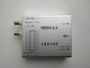
Instrustar MDSO-LA
Jump to navigation
Jump to search
The printable version is no longer supported and may have rendering errors. Please update your browser bookmarks and please use the default browser print function instead.
 | |
| Status | supported |
|---|---|
| Channels | 2 |
| Samplerate | 48MHz |
| Analog bandwidth | 20MHz |
| Vertical resolution | 8bit |
| Triggers | none (SW-only) |
| Input impedance | 1MΩ‖25pF |
| Memory | none |
| Display | none |
| Connectivity | USB |
| Website | instrustar.com |
The Instrustar MDSO-LA is a USB-based, same hardware as YiXingDianZi MDSO except that add the logic analyzer and a double eeprom to provide 2 different VID/PID.
- 2-channel oscilloscope with an analog bandwidth of 20MS/s and 48MS/s sampling rate,
- 8/16-channel logic analyzer with a max. sampling rate of 24MHz.
Hardware
- USB: Cypress CY7C68013A-100AXC (FX2LP) (datasheet)
- 256-byte I²C EEPROM: 2x Microchip 24LC02BI (datasheet)
- 16-Bit bus transceiver with 3-state outputs: TI SN74LVC16245A (datasheet)
- 8-channel analog mux/demux: 2x NXP 74HC4051D (datasheet)
- 1A low-dropout voltage regulator (3.3V): Advanced Monolithic Systems AMS1117-3.3 datasheet)
- 2W, fixed input, isolated & unregulated dual/single output DC/DC converter: Mornsun A_S-2WR2 (A0505S-2WR2) (datasheet)
- ADC 8-bit, 40MHz, dual ADC: Analog Devices AD9288 (datasheet)
- 1.4GHz current feedback amplifiers with enable: 2x Intersil EL5166 (datasheet)
- 145 MHz FastFET Opamps: 2x AD8065: (datasheet), markings "HRA"
- Crystal: 24MHz
The device has a switch. Depending on the position it comes up with different USB VID/PIDs:
- MDSO-LA: See YiXingDianZi MDSO/Info for more details (such as lsusb -v output) on the device (used for oscilloscope mode).
- Saleae Logic: 0925:3881 Lakeview Research Saleae Logic (Saleae Logic VID/PID, so fx2lafw works out of the box)
Cypress FX2 pinout:
| PD5 | 1- | O | -56 | PD4 |
| PD6 | 2- | -55 | PD3 | |
| PD7 | 3- | -54 | PD2 | |
| GND | 4- | -53 | PD1 | |
| CLKOUT | 5- | -52 | PD0 | |
| VCC | 6- | -51 | *WAKEUP | |
| GND | 7- | -50 | VCC | |
| RDY0/*SLRD | 8- | -49 | RESET# | |
| RDY1/*SLWR | 9- | -48 | GND | |
| AVCC | 10- | -47 | PA7 (Activate analog mode vs digital mode) | |
| (24MHz crystal) XTALOUT | 11- | -46 | PA6 (74HC4051, S2) | |
| (24MHz crystal) XTALIN | 12- | -45 | PA5 (74HC4051, S1) | |
| AGND | 13- | -44 | PA4 (74HC4051, S0) | |
| AVCC | 14- | -43 | PA3 (74HC4051, S0) | |
| (USB D+) DPLUS | 15- | -42 | PA2 (774HC4051, S1) | |
| (USB D-) DMINUS | 16- | -41 | PA1 (74HC4051, S2) | |
| AGND | 17- | -40 | PA0 | |
| VCC | 18- | -39 | VCC | |
| GND | 19- | -38 | CTL2 | |
| (CTL0, AD9288 ENCA/B) *IFCLK | 20- | -37 | CTL1 | |
| RESERVED | 21- | -36 | CTL0 (IFCLK, AD9288 ENCA/B) | |
| (EEPROM SCL) SCL | 22- | -35 | GND | |
| (EEPROM SDA) SDA | 23- | -34 | VCC | |
| VCC | 24- | -33 | GND | |
| PB0 | 25- | -32 | PB7 | |
| PB1 | 26- | -31 | PB6 | |
| PB2 | 27- | -30 | PB5 | |
| PB3 | 28- | -29 | PB4 |
NXP 74HC4051D (upper/lower, CH1/CH2) pinout:
|
|
Microchip 24LC02B (top / bottom) pinout: There are 2 for the 2 possible hardware configurations (as MSDO-LA or as USBee)
|
Analog Devices AD9288 pinout:
| AD9288 pins | Description |
|---|---|
| S1, S2 | S1=VCC, S2=GND. "Normal operation, data align disabled". |
| DFS | Tied to GND. Data format select = "offset binary" (not "twos complement"). |
| AINA, AINB | Analog input channels. |
| D0A-D7A | Connected to FX2 PB0-PB7. |
| D0B-D7B | Connected to FX2 PD0-PD7. |

