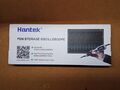
Hantek PSO2020
Jump to navigation
Jump to search
The printable version is no longer supported and may have rendering errors. Please update your browser bookmarks and please use the default browser print function instead.
 | |
| Status | |
|---|---|
| Source code | [1] |
| Channels | 1 |
| Samplerate | 96MHz |
| Analog bandwidth | 20MHz |
| Vertical resolution | 8bit |
| Triggers | none (SW-only) |
| Input impedance | 1MΩ‖25pF |
| Memory | none |
| Display | none |
| Connectivity | USB |
| Website | hantek.com |
The Hantek PSO2020 is a USB-based, 1-channel oscilloscope with an analog bandwidth of 20MS/s and 96MS/s sampling rate. Wide input rage, from ±100mV to ±50V.
See Hantek PSO2020/Info for more details (such as lsusb -v output) about the device.
Hardware
- USB: Cypress CY7C68013A-100AXC (FX2LP) (datasheet)
- 256-byte I²C EEPROM: Microchip 24LC02BI (datasheet)
- 1x 8-channel analog multiplexer/demultiplexer (U6): NXP 74HC4051D (datasheet)
- 1A low-dropout voltage regulator (3.3V): Advanced Monolithic Systems AMS1117-3.3 (datasheet)
- ?? 2W, fixed input, isolated & unregulated dual/single output DC/DC converter: Mornsun A_S-2WR2 (A0505S-2WR2) (datasheet)
- 8-bit, 40/80/100MHz, dual ADC: Analog Devices AD9288 (datasheet)
- ?? 4x 145 MHz FastFET Op Amp: Analog Devices AD8065 (datasheet)
- Crystal: 24MHz
- 1x Photocoupler (U100): Toshiba TPL280 (datasheet)
- 1x 4.5V Relay (used for High Voltage selection - U10): NEC UD2-4.5NU (datasheet)
- 1x ±5V DC/DC Coverter (U13): INOUT A0505S (datasheet)
Microchip 24LC02BI pinout:
| (Low, but not GND) A0 | 1- | O | -8 | VCC |
| (GND) A1 | 2- | -7 | WP (GND) | |
| (GND) A2 | 3- | -6 | SCL (FX2 SCL) | |
| VSS | 4- | -5 | SDA (FX2 SDA) |
Analog Devices ADS9288 pinout:
| AD9288 pins | Description |
|---|---|
| S1, S2 | Tied to VCC. "Data Align Enabled (data from both channels available on rising edge of Clock A. Channel B data is delayed a 1/2 clock cycle).". |
| DFS | Tied to GND. Data format select = "offset binary" (not "twos complement"). |
| REF_IN_A, REF_IN_B | Tied to REF_OUT. |
| AINA, AINB | Analog input channels. |
Cypress FX2 pinout:
| FX2 pins | Description |
|---|---|
| CTL0 | Connected to AD9288 ENCA, to ENCB with an inverter. and to FX2 IFCLK. |
| PB0-PB7 | Connected to AD9288 D7A-D0A. Bit reversed! Must be reversed back in software. |
| PD0-PD7 | Connected to AD9288 D0B-D7B. |
| PA0, PA1, PA5 (Inputs) | Connected to the 3 buttons |
| PC0, PC3, PE?, PE? (Inputs) | Connected to the front selector |
| PC1 | Connected to S1 of the 74HC4051D mux |
| PC2 | Connected to S0 of the 74HC4051D mux |
| PC4 | AC/DC Selector |
| PA7 | Voltage Selection Relay |
| PA6 | Green LED |
| PE1 | Front light |
| PE2 | Red LED |
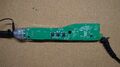
Photos
Box Front

Box Back
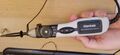
Device
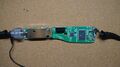
Inside Front
Inside Back
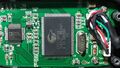
Inside Detail
- Error creating thumbnail: Unable to save thumbnail to destination
Analog input section


Protocol
Firmware
Note: The firmware is not flashed into the device permanently! It will be automatically "uploaded" to the Cypress FX2's SRAM every time you attach the device to a USB port.
EEPROM layout
The device has a 256-byte I²C EEPROM with the following layout:
c0 b4 04 23 60 00 00 00 91 91 91 91 8a 8a 85 85
81 81 91 91 8a 8a 85 81 81 81 81 81 91 91 91 91
8a 8a 85 85 81 81 91 91 8a 8a 85 81 81 81 81 81
ff ff ff ff ff ff ff ff ff ff ff ff ff ff ff ff
ff ff ff ff ff ff ff ff ff ff ff ff ff ff ff ff
ff ff ff ff ff ff ff ff ff ff ff ff ff ff ff ff
ff ff ff ff ff ff ff ff ff ff ff ff ff ff ff ff
ff ff ff ff ff ff ff ff ff ff ff ff ff ff ff ff
ff ff ff ff ff ff ff ff ff ff ff ff ff ff ff ff
ff ff ff ff ff ff ff ff ff ff ff ff ff ff ff ff
ff ff ff ff ff ff ff ff ff ff ff ff ff ff ff ff
ff ff ff ff ff ff ff ff ff ff ff ff ff ff ff ff
ff ff ff ff ff ff ff ff ff ff ff ff ff ff ff ff
ff ff ff ff ff ff ff ff ff ff ff ff ff ff ff ff
ff ff ff ff ff ff ff ff ff ff ff ff ff ff ff ff
ff ff ff ff ff ff ff ff ff ff ff ff ff ff ff ff
Description:
| Bytes | Description |
|---|---|
| 0 | 0xc0: FX2 "c0 load" mode, i.e. VID/PID/DID are loaded from EEPROM (but not firmware). |
| 1-2 | 0x04b4: USB vendor ID (VID). |
| 3-4 | 0x6023: USB product ID (PID). |
| 5-6 | 0x0000: USB device ID (DID). |
| 7 | 0x00: FX2 configuration byte (see FX2 TRM for details). |
| 8-47 | Unknown. Possibly calibration data? |
| 48-255 | All-0xff. |