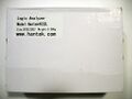
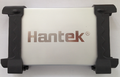
Hantek 4032L
Jump to navigation
Jump to search
The printable version is no longer supported and may have rendering errors. Please update your browser bookmarks and please use the default browser print function instead.
 | |
| Status | supported |
|---|---|
| Source code | hantek-4032l |
| Channels | 32 |
| Samplerate | 400MHz |
| Samplerate (state) | ? |
| Triggers | edge, bus value range, pattern, pattern duration, combined |
| Min/max voltage | -6V — +60V input, -6V — +6V threshold |
| Memory | 2Gbit (64M samples x 32) |
| Compression | — |
| Website | hantek.com |
The Hantek 4032L is a USB-based, 32-channel logic analyzer with up to 400MHz sampling rate and 2Gbit DDR2 memory.
See Hantek 4032L/Info for more details (such as lsusb -v output) on the device.
Hardware
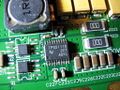
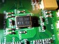
- Xilinx Spartan-6 XC6SLX16 CSG324 DIV1225 (FPGA, 14579 logic cells, 2 DDR1/2/3 memory controllers, BGA324)
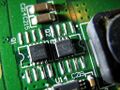
- Cypress FX2LP CY7C68013A-100AXC (USB 2.0 HS controller, TQFP100)
- 2x Micron MT47H64M16HR-25E:H (1Gbit DDR2 SDRAM, BGA)
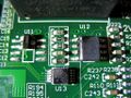
- TI TPS51116 (DDR memory power controller)
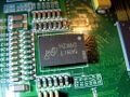
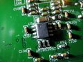
- Unknown I2C EEPROM (marking removed, contains FX2 firmware)
- MXIC MX25L4005 (4Mbit SPI flash, marking removed, contains FPGA bitstream)
- DAC122S085CIMM (marking removed, input Vref generators)
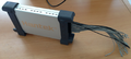
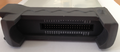
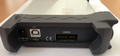
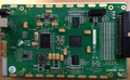
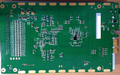
Photos
Teardown 1:
Package
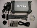
Package contents
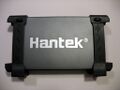
Device, top
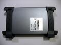
Device, bottom
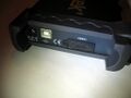
USB connector
Probe connector
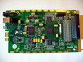
PCB, top
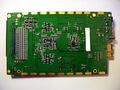
PCB, bottom
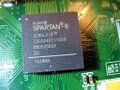
Xilinx XC6SLX16
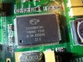
Cypress FX2
DDR2 SDRAM
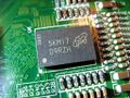
DDR2 SDRAM
TI TPS51116
TI TPS54286
SPI flash
Mornsun A0512S-1WR2
50MHz crystal
Unknown chips
Unknown chips
Unknown chips


Teardown 2:
Device, top
Device, with probes
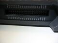
Probe port side
PC USB port side
PCB, top
PCB, bottom


Protocol
- Vendor request is used to reset the engine and flush the buffers
- Endpoint 2 is used for host-to-device command/parameters transfers
- Endpoint 6 is used for device-to-host status/data transfers
X denotes "any value" in the following description
Vendor requests
- bRequest=0xB3, wValue=X, wIndex=X, wLength=0x0A, data={ 0x0F, 0x03, 0x03, 0x03, X, X, X, X, X, X } - restart the engine (reset FPGA, reset FIFOs)
- bRequest=0xD0, wValue=X, wIndex=X, wLength=0x00 - disable communication (set FIFO reset), not used
- bRequest=0xD1, wValue=X, wIndex=X, wLength=0x00 - enable communication (clear FIFO reset), not used
Command/Parameters packet
 struct CmdParamsPacket

   byte Magic[2]={ 0x7F, 0x01 }

   byte SampleRate
     0x22 - 400MS/s
     0x23 - 320MS/s
     0x20 - 200MS/s
     0x21 - 160MS/s
     0x00 - 100MS/s
     0x08 - 80MS/s
     0x01 - 50MS/s
     0x09 - 40MS/s
     0x02 - 25MS/s
     0x0A - 20MS/s
     0x03 - 12.5MS/s
     0x0B - 10MS/s
     0x04 - 6.25MS/s
     0x0C - 5MS/s
     0x10 - 4MS/s
     0x05 - 3.125MS/s
     0x0D - 2.5MS/s
     0x11 - 2MS/s
     0x06 - 1.5625MS/s
     0x0E - 1.25MS/s
     0x12 - 1MS/s
     0x07 - 781.25KS/s
     0x0F - 625KS/s
     0x13 - 500KS/s
     0x14 - 250KS/s
     0x15 - 125KS/s
     0x16 - 62.5KS/s
     0x17 - 31.25KS/s
     0x18 - 16KS/s
     0x19 - 8KS/s
     0x1A - 4KS/s
     0x1B - 2KS/s
     0x1C - 1KS/s
     0x24 - posedge CLKA
     0x25 - posedge CLKB
     0x28 - negedge CLKA
     0x29 - negedge CLKB
     0x26 - DDR CLKA
     0x27 - DDR CLKB

   byte TrigFlags
     bit 0 - enable trigger 1 (main)
     bit 1 - enable trigger 2 (advanced)
     bit 2 - trigger logic, 0 - T1 or T2, 1 - T1 and T2
     bit 3 - unknown USBXI sync trigger config, default: 1
     bit 4 - unknown USBXI sync trigger config, default: 0
     bit 7 - unknown USBXI "check mode", default: 0

   word PwmA - channel A Vref PWM value, pseudocode:
     -6V < ThresholdVoltage < +6V
     Vref = 1.8-ThresholdVoltage
     if Vref>10.0
       Vref = 10.0
     if Vref<-5.0
       Vref = -5.0
     pwm = ToInt((Vref + 5.0) / 15.0 * 4096.0)
       if pwm>4095
       pwm = 4095

   word PwmB - channel B Vref PWM value

   byte UsbxiData - unknown USBXI parameter, default: 00

   byte unused: 00

   dword SampleDepth - sample depth in bits per channel, 2k-64M, must be multiple of 512

   dword PretriggerDepth - pretrigger buffer depth in bits, must be < SampleDepth

   struct Trig Trig1 - trigger 1 config, see below

   struct Trig Trig2 - trigger 2 config, see below

   byte Command[2] - command, see Commands and responses below
 struct Trig

   dword Flags - trigger types selection:
     bit 4:0 - edge trigger signal, 0-31 -> A0-B15
     bit 6:5 - edge to trigger on:
       00 - rise
       01 - fall
       10 - rise or fall
       11 - edge trigger disabled
     bit 7 - unused
     bit 9:8 - data range trigger type:
       00 - data=RangeMax trigger
       01 - data=RangeMin or data=RangeMax trigger
       10 - data<RangeMin or data>RangeMax trigger
       11 - RangeMin<data<RangeMax trigger
     bit 11:10 - time range trigger type:
       00 - time=TimeMax trigger
       01 - time=TimeMin or time=TimeMax trigger
       10 - time<TimeMin or time>TimeMax trigger
       11 - TimeMin<time<TimeMax trigger
     bit 12 - enable data range trigger (see bit 9:8)
     bit 13 - enable time trigger (see bit 11:10)
     bit 15:14 - unused
     bit 17:16 - combined trigger data selection (data=EquData and data_sel matches other criteria like time, range, edge):
       00 - data_sel is next data (next to matched with EquData)
       01 - data_sel is current data
       10 - data_sel is previous data
       11 - undefined
     bit 18 - enable combined trigger (see bit 17:16)
     bit 31:19 - unused

   dword RangeMin - min value for data range trigger (see Flags[9:8]), must be masked with RangeMask (see Masking below)

   dword RangeMax - max value for data range trigger (see Flags[9:8]), must be masked with RangeMask

   dword TimeMin - min value for time trigger (see Flags[11:10])

   dword TimeMax - max value for time trigger (see Flags[11:10])

   dword RangeMask - mask value for data range trigger

   dword EquMask - mask value for combined trigger

   dword EquData - data value for combined trigger (see Flags[17:16]), must be masked with EquMask
 Masking:
   Some trigger types (data range, combined "pattern and condition") operate on a "bus" value of several signals selected with a mask. Active bits are combined to a single value WITHOUT GAPS:
     mask=01000011, value=11010001 -> masked_value=00000101 (bits 6,1,0 are combined and zero-extended)
Commands and responses
 { 0x1A, 0x2B } - configure and start capture, all parameters are used
 Response: none
 { 0x3A, 0x4B } - get status, parameters are defaults
 Response:
   dword Magic=0x2B1A037F - drop rx data until this)
   dword CurrentDataValue - A0-B15 current state snapshot
   dword CaptureStatus - 0-not finished, 1-?, 2-done, data is ready
   dword UsbxiData - unknown USBXI data
   dword DevVersion - FPGA firmware version
   dword DummyData[251] - pad to 1024 bytes
 { 0x5A, 0x6B } - get captured data, parameters are defaults
 Response:
   dword Magic=0x2B1A027F - drop rx data until this
   dword CaptureData[SampleDepth] - capture data
   dword EndMarker=0x4D3C037F - drop rx data after this till end of 512 byte packet
 { 0x9A, 0xAB } - unknown USBXI "eraser data" cmd, parameters are defaults
 Response: none
 { 0xBA, 0xCB } - unknown USBXI "set sync trig output" cmd, parameters are defaults
 Response: none
Acquisition session flow
- Send restart vendor request (0xB3)
- Send { 0x1A, 0x2B } type packet to configure and start capture
- Poll with { 0x3A, 0x4B } until CaptureStatus=2 (optionally blink bus indicators according to CurrentDataValue during poll)
- Get capture data with { 0x5A, 0x6B }
Hardware features support status
 + Buffered mode acquisition
 + Sample depth selection
 + Pretrigger depth selection
 + Internal clocking (timing mode)
 + External clocking (state mode) with edge (rising/falling/both) and clock channel (ACLK/BCLK) selection
 + Logic voltage threshold selection (independent for Axx and Bxx channel groups, possible to analyze dual standard circuits)
 + Unconditional trigger
 + Trigger on signal edge (rising/falling/any)
 + Trigger on bus pattern match
 - Trigger on bus value within/out of range
 - Trigger on bus pattern condition (match/within/out of range) repeating for N consecutive samples
   where N is equal/within range/out of range
 - Trigger on bus pattern condition at specific signal edge
 - Trigger on any of the above conditions combined with pattern match on the previous/current/next sample
 - Use two trigger units in AND/OR combination
 - External trigger input/output signals