Hantek PSO2020
Revision as of 12:20, 23 December 2017 by Martinloren (talk | contribs) (Created page with "{{Infobox oscilloscope | image = 180px | name = Hantek PSO2020 | channels = 1 | samplerate...")
| File:Hantek PSO2020 mugshot.png | |
| Status | |
|---|---|
| Source code | [1] |
| Channels | 1 |
| Samplerate | 96MHz |
| Analog bandwidth | 20MHz |
| Vertical resolution | 8bit |
| Triggers | none (SW-only) |
| Input impedance | 1MΩ‖25pF |
| Memory | none |
| Display | none |
| Connectivity | USB |
| Website | hantek.com |
The Hantek PSO2020 is a USB-based, 1-channel oscilloscope with an analog bandwidth of 20MS/s and 96MS/s sampling rate.
See Hantek PSO2020/Info for more details (such as lsusb -v output) about the device.
Hardware
- USB: Cypress CY7C68013A-100AXC (FX2LP) (datasheet)
- 256-byte I²C EEPROM: Microchip 24LC02BI (datasheet)
- 2x 8-channel analog multiplexer/demultiplexer: NXP 74HC4051D (datasheet)
- 1A low-dropout voltage regulator (3.3V): Advanced Monolithic Systems AMS1117-3.3 (datasheet)
- 2W, fixed input, isolated & unregulated dual/single output DC/DC converter: Mornsun A_S-2WR2 (A0505S-2WR2) (datasheet)
- 8-bit, 40/80/100MHz, dual ADC: Analog Devices AD9288 (datasheet)
- 4x 145 MHz FastFET Op Amp: Analog Devices AD8065 (datasheet)
- Crystal: 24MHz
NXP 74HC4051D (upper/lower, CH1/CH2) pinout:
|
|
| S2 | S1 | S0 | 74HC4051D Mux | VDIVs (vendor software) |
|---|---|---|---|---|
| 0 | 0 | 0 | Y0 to Z | 200mV |
| 0 | 0 | 1 | Y1 to Z | 500mV |
| 0 | 1 | 0 | Y2 to Z | 5V, 2V, 1V |
| 0 | 1 | 1 | Y3 to Z | 100mV, 50mV, 20mV |
Microchip 24LC02BI pinout:
| (Low, but not GND) A0 | 1- | O | -8 | VCC |
| (GND) A1 | 2- | -7 | WP (GND) | |
| (GND) A2 | 3- | -6 | SCL (FX2 SCL) | |
| VSS | 4- | -5 | SDA (FX2 SDA) |
Analog Devices ADS9288 pinout:
| AD9288 pins | Description |
|---|---|
| S1, S2 | S1=VCC, S2=GND. "Normal operation, data align disabled". |
| DFS | Tied to GND. Data format select = "offset binary" (not "twos complement"). |
| AINA, AINB | Analog input channels. |
Cypress FX2 pinout:
| FX2 pins | Description | |||||||||||||||
|---|---|---|---|---|---|---|---|---|---|---|---|---|---|---|---|---|
| CTL2 | Connected to AD9288 ENCA and ENCB and FX2 IFCLK. | |||||||||||||||
| PB0-PB7 | Connected to AD9288 D0A-D7A. | |||||||||||||||
| PD0-PD7 | Connected to AD9288 D0B-D7B. | |||||||||||||||
| PA7 | 1kHz probe calibration pin. | |||||||||||||||
| PC0/PC1 | Dual-color (red/green) LED.
|
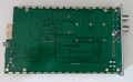
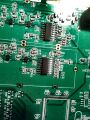
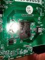
Photos
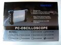
Box
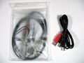
Accessories


Another teardown:
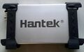
Device, top
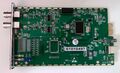
PCB, top
PCB, bottom
Feedback resistor selector
Cypress FX2LP


Protocol
| Oscilloscope command | bRequest value | Notes |
|---|---|---|
| Set CH0 voltage range | 0xE0 | Possible values: 1, 2, 5, 10 (5V, 2.5V, 1V, 500mV). |
| Set CH1 voltage range | 0xE1 | Possible values: 1, 2, 5, 10 (5V, 2.5V, 1V, 500mV). |
| Set sampling rate | 0xE2 | Possible values: 48, 30, 24, 16, 8, 4, 1 (MHz) and 50, 20, 10 (*10kHz). |
| Trigger oscilloscope | 0xE3 | Possible values: 1 == start sampling. 0 == ignored currently. |
| Set number of channels | 0xE4 | Possible values: 1, 2. |
Firmware
Note: The firmware is not flashed into the device permanently! It will be automatically "uploaded" to the Cypress FX2's SRAM every time you attach the device to a USB port.