Difference between revisions of "Instrustar MDSO-LA"
Jump to navigation
Jump to search
Martinloren (talk | contribs) m |
Martinloren (talk | contribs) m (→Hardware) |
||
| (One intermediate revision by the same user not shown) | |||
| Line 27: | Line 27: | ||
* '''256-byte I²C EEPROM''': 2x [http://www.microchip.com/wwwproducts/en/24LC02B Microchip 24LC02BI] ([http://ww1.microchip.com/downloads/en/DeviceDoc/21709J.pdf datasheet]) | * '''256-byte I²C EEPROM''': 2x [http://www.microchip.com/wwwproducts/en/24LC02B Microchip 24LC02BI] ([http://ww1.microchip.com/downloads/en/DeviceDoc/21709J.pdf datasheet]) | ||
* '''16-Bit bus transceiver with 3-state outputs''': [http://www.ti.com/product/sn74lvc16245a TI SN74LVC16245A] ([http://www.ti.com/lit/ds/symlink/sn74lvc16245a.pdf datasheet]) | * '''16-Bit bus transceiver with 3-state outputs''': [http://www.ti.com/product/sn74lvc16245a TI SN74LVC16245A] ([http://www.ti.com/lit/ds/symlink/sn74lvc16245a.pdf datasheet]) | ||
* '''8-channel analog mux/demux''': 2x [http://www.nxp.com/products/discretes-and-logic/logic/8-channel-analog-multiplexer-demultiplexer:74HC4051D NXP 74HC4051D] ([ | * '''8-channel analog mux/demux''': 2x [http://www.nxp.com/products/discretes-and-logic/logic/8-channel-analog-multiplexer-demultiplexer:74HC4051D NXP 74HC4051D] ([https://assets.nexperia.com/documents/data-sheet/74HC_HCT4051.pdf datasheet]) | ||
* '''1A low-dropout voltage regulator (3.3V):''' [http://www.advanced-monolithic.com/products/voltreg.html#1117 Advanced Monolithic Systems AMS1117-3.3] [http://www.advanced-monolithic.com/pdf/ds1117.pdf datasheet]) | * '''1A low-dropout voltage regulator (3.3V):''' [http://www.advanced-monolithic.com/products/voltreg.html#1117 Advanced Monolithic Systems AMS1117-3.3] [http://www.advanced-monolithic.com/pdf/ds1117.pdf datasheet]) | ||
* '''2W, fixed input, isolated & unregulated dual/single output DC/DC converter''': [http://www.mornsun.cn/html/product/content/A_S-2WR2.html Mornsun A_S-2WR2 (A0505S-2WR2)] ([http://www.mornsun.cn/uploads/pdf/A_S-2WR2.pdf datasheet]) | * '''2W, fixed input, isolated & unregulated dual/single output DC/DC converter''': [http://www.mornsun.cn/html/product/content/A_S-2WR2.html Mornsun A_S-2WR2 (A0505S-2WR2)] ([http://www.mornsun.cn/uploads/pdf/A_S-2WR2.pdf datasheet]) | ||
| Line 213: | Line 213: | ||
[[Category:Oscilloscope]] | [[Category:Oscilloscope]] | ||
[[Category:Logic analyzer]] | [[Category:Logic analyzer]] | ||
[[Category: | [[Category:Supported]] | ||
Latest revision as of 11:51, 19 February 2019
 | |
| Status | supported |
|---|---|
| Channels | 2 |
| Samplerate | 48MHz |
| Analog bandwidth | 20MHz |
| Vertical resolution | 8bit |
| Triggers | none (SW-only) |
| Input impedance | 1MΩ‖25pF |
| Memory | none |
| Display | none |
| Connectivity | USB |
| Website | instrustar.com |
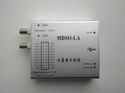
The Instrustar MDSO-LA is a USB-based, same hardware as YiXingDianZi MDSO except that add the logic analyzer and a double eeprom to provide 2 different VID/PID.
- 2-channel oscilloscope with an analog bandwidth of 20MS/s and 48MS/s sampling rate,
- 8/16-channel logic analyzer with a max. sampling rate of 24MHz.
Hardware
- USB: Cypress CY7C68013A-100AXC (FX2LP) (datasheet)
- 256-byte I²C EEPROM: 2x Microchip 24LC02BI (datasheet)
- 16-Bit bus transceiver with 3-state outputs: TI SN74LVC16245A (datasheet)
- 8-channel analog mux/demux: 2x NXP 74HC4051D (datasheet)
- 1A low-dropout voltage regulator (3.3V): Advanced Monolithic Systems AMS1117-3.3 datasheet)
- 2W, fixed input, isolated & unregulated dual/single output DC/DC converter: Mornsun A_S-2WR2 (A0505S-2WR2) (datasheet)
- ADC 8-bit, 40MHz, dual ADC: Analog Devices AD9288 (datasheet)
- 1.4GHz current feedback amplifiers with enable: 2x Intersil EL5166 (datasheet)
- 145 MHz FastFET Opamps: 2x AD8065: (datasheet), markings "HRA"
- Crystal: 24MHz
The device has a switch. Depending on the position it comes up with different USB VID/PIDs:
- MDSO-LA: See YiXingDianZi MDSO/Info for more details (such as lsusb -v output) on the device (used for oscilloscope mode).
- Saleae Logic: 0925:3881 Lakeview Research Saleae Logic (Saleae Logic VID/PID, so fx2lafw works out of the box)
Cypress FX2 pinout:
| PD5 | 1- | O | -56 | PD4 |
| PD6 | 2- | -55 | PD3 | |
| PD7 | 3- | -54 | PD2 | |
| GND | 4- | -53 | PD1 | |
| CLKOUT | 5- | -52 | PD0 | |
| VCC | 6- | -51 | *WAKEUP | |
| GND | 7- | -50 | VCC | |
| RDY0/*SLRD | 8- | -49 | RESET# | |
| RDY1/*SLWR | 9- | -48 | GND | |
| AVCC | 10- | -47 | PA7 (Activate analog mode vs digital mode) | |
| (24MHz crystal) XTALOUT | 11- | -46 | PA6 (74HC4051, S2) | |
| (24MHz crystal) XTALIN | 12- | -45 | PA5 (74HC4051, S1) | |
| AGND | 13- | -44 | PA4 (74HC4051, S0) | |
| AVCC | 14- | -43 | PA3 (74HC4051, S0) | |
| (USB D+) DPLUS | 15- | -42 | PA2 (774HC4051, S1) | |
| (USB D-) DMINUS | 16- | -41 | PA1 (74HC4051, S2) | |
| AGND | 17- | -40 | PA0 | |
| VCC | 18- | -39 | VCC | |
| GND | 19- | -38 | CTL2 | |
| (CTL0, AD9288 ENCA/B) *IFCLK | 20- | -37 | CTL1 | |
| RESERVED | 21- | -36 | CTL0 (IFCLK, AD9288 ENCA/B) | |
| (EEPROM SCL) SCL | 22- | -35 | GND | |
| (EEPROM SDA) SDA | 23- | -34 | VCC | |
| VCC | 24- | -33 | GND | |
| PB0 | 25- | -32 | PB7 | |
| PB1 | 26- | -31 | PB6 | |
| PB2 | 27- | -30 | PB5 | |
| PB3 | 28- | -29 | PB4 |
NXP 74HC4051D (upper/lower, CH1/CH2) pinout:
|
|
Microchip 24LC02B (top / bottom) pinout: There are 2 for the 2 possible hardware configurations (as MSDO-LA or as USBee)
|
Analog Devices AD9288 pinout:
| AD9288 pins | Description |
|---|---|
| S1, S2 | S1=VCC, S2=GND. "Normal operation, data align disabled". |
| DFS | Tied to GND. Data format select = "offset binary" (not "twos complement"). |
| AINA, AINB | Analog input channels. |
| D0A-D7A | Connected to FX2 PB0-PB7. |
| D0B-D7B | Connected to FX2 PD0-PD7. |

