Difference between revisions of "Sysclk LWLA1034"
Jump to navigation
Jump to search
(Fill in some more Infobox details) |
(Link to correct item on AliExpress) |
||
| (6 intermediate revisions by 3 users not shown) | |||
| Line 2: | Line 2: | ||
| image = [[File:Sysclk lwla1034 mugshot.png|180px]] | | image = [[File:Sysclk lwla1034 mugshot.png|180px]] | ||
| name = Sysclk LWLA1034 | | name = Sysclk LWLA1034 | ||
| status = | | status = supported | ||
| source_code_dir = | | source_code_dir = sysclk-lwla | ||
| channels = 34 | | channels = 34 | ||
| samplerate = 125MHz (max) | | samplerate = 125MHz (max) | ||
| Line 12: | Line 12: | ||
| memory = 256Kbit/channel | | memory = 256Kbit/channel | ||
| compression = RLE | | compression = RLE | ||
| website = [http:// | | website = [http://www.aliexpress.com/item/free-shipping-New-arrival-Powerful-100MHz-34-channels-LA1034-Logic-Analyzer-Timing-State-Logic-Analyzer/1227957767.html aliexpress.com] | ||
}} | }} | ||
| Line 24: | Line 24: | ||
* Cypress CY7C68013A-56 (FX2) USB interface chip | * Cypress CY7C68013A-56 (FX2) USB interface chip | ||
* Cypress 256k×36 SRAM (likely a [http://www.cypress.com/?mpn=CY7C1361C-133AXC CY7C1361C-133AXC] or similar) | * Cypress 256k×36 SRAM (likely a [http://www.cypress.com/?mpn=CY7C1361C-133AXC CY7C1361C-133AXC] or similar) | ||
* STC15F104E 8051-based microcontroller | |||
The not-installed 10-pin connector between the USB socket and the large capacitor seems to connect to the JTAG pins of the FPGA. | |||
== Photos == | == Photos == | ||
<gallery> | |||
File:Sysclk lwla1034 device top.jpg | |||
File:Sysclk lwla1034 device bottom.jpg | |||
File:Sysclk lwla1034 device connector.jpg | |||
File:Sysclk lwla1034 device usb.jpg | |||
File:Sysclk lwla1034 device open.jpg | |||
File:Sysclk lwla1034 pcb top2.jpg | |||
File:Sysclk lwla1034 pcb bottom2.jpg | |||
File:Sysclk lwla1034 altera cyclone2.jpg | |||
File:Sysclk lwla1034 cypress sram.jpg | |||
File:Sysclk lwla1034 cypress fx2.jpg | |||
File:Sysclk lwla1034 24c64n otherso8 crystal.jpg | |||
File:Sysclk lwla1034 crystal 50mhz.jpg | |||
File:Sysclk lwla1034 crystal 40mhz.jpg | |||
File:Sysclk lwla1034 ams1117 33.jpg | |||
File:Sysclk lwla1034 ams1117 12.jpg | |||
</gallery> | |||
(Note: The yellow/greenish markings weren't there, they're added by the photographer) | |||
''' PCB for another device''': | |||
<gallery> | <gallery> | ||
File:Sysclk lwla1034 pcb top.jpg|<small>PCB, top</small> | File:Sysclk lwla1034 pcb top.jpg|<small>PCB, top</small> | ||
| Line 34: | Line 58: | ||
File:Sysclk lwla1034 chip3 removed marking.jpg|<small>SRAM (marking removed)</small> | File:Sysclk lwla1034 chip3 removed marking.jpg|<small>SRAM (marking removed)</small> | ||
</gallery> | </gallery> | ||
== Software == | == Software == | ||
| Line 43: | Line 65: | ||
== Firmware == | == Firmware == | ||
* The FX2 firmware | We have received permission from the vendor to distribute the FPGA bitstreams with sigrok. Thus, the bitstreams are now included in the sigrok-firmware module. | ||
* Endpoint 4 | |||
* Endpoint 2 is | * The FX2 firmware is loaded from an EEPROM on the board, so that the final USB device descriptor is immediately available on power-up. | ||
* Endpoint 4 is used exclusively for loading a new bitstream into the FPGA. | |||
* Endpoint 2 is used for sending commands to the FPGA firmware, with responses (if any) coming in from endpoint 6. | |||
Reverse engineering of the vendor protocol | Reverse engineering of the vendor's custom protocol has been completed. See [[Sysclk LWLA1034/Protocol]] for the documentation. | ||
== Resources == | == Resources == | ||
| Line 55: | Line 79: | ||
[[Category:Device]] | [[Category:Device]] | ||
[[Category:Logic analyzer]] | [[Category:Logic analyzer]] | ||
[[Category: | [[Category:Supported]] | ||
Latest revision as of 22:27, 28 February 2014
 | |
| Status | supported |
|---|---|
| Source code | sysclk-lwla |
| Channels | 34 |
| Samplerate | 125MHz (max) |
| Samplerate (state) | ? |
| Triggers | 34 + extern |
| Min/max voltage | 0-5V |
| Threshold voltage | ? |
| Memory | 256Kbit/channel |
| Compression | RLE |
| Website | aliexpress.com |
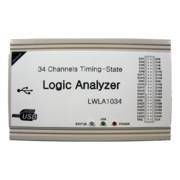
The Sysclk LWLA1034 is a USB-based, 34-channel logic analyzer with up to 125MHz sampling rate.
See Sysclk LWLA1034/Info for more details (such as lsusb -v output) about the device.
Hardware
- Altera EP2C5Q208C8N (Cyclone II) FPGA
- Cypress CY7C68013A-56 (FX2) USB interface chip
- Cypress 256k×36 SRAM (likely a CY7C1361C-133AXC or similar)
- STC15F104E 8051-based microcontroller
The not-installed 10-pin connector between the USB socket and the large capacitor seems to connect to the JTAG pins of the FPGA.
Photos
(Note: The yellow/greenish markings weren't there, they're added by the photographer)
PCB for another device:
Software
Firmware
We have received permission from the vendor to distribute the FPGA bitstreams with sigrok. Thus, the bitstreams are now included in the sigrok-firmware module.
- The FX2 firmware is loaded from an EEPROM on the board, so that the final USB device descriptor is immediately available on power-up.
- Endpoint 4 is used exclusively for loading a new bitstream into the FPGA.
- Endpoint 2 is used for sending commands to the FPGA firmware, with responses (if any) coming in from endpoint 6.
Reverse engineering of the vendor's custom protocol has been completed. See Sysclk LWLA1034/Protocol for the documentation.


