Difference between revisions of "XMOS XTAG-2"
Jump to navigation
Jump to search
(add xtag2 photos) |
m (replace jpeg by png with transparency background) |
||
| Line 28: | Line 28: | ||
<gallery> | <gallery> | ||
File:Xtag-2 front. | File:Xtag-2 front.png|<small>PCB, front</small> | ||
File:Xtag-2 back.jpeg|<small>PCB, back</small> | File:Xtag-2 back.jpeg|<small>PCB, back</small> | ||
</gallery> | </gallery> | ||
Revision as of 10:32, 4 January 2014
 | |
| Status | planned |
|---|---|
| Channels | ???? |
| Samplerate | 50MHz @ 2ch, 16MHz @ 7ch |
| Samplerate (state) | ? |
| Triggers | ? |
| Min/max voltage | ? |
| Threshold voltage | ? |
| Memory | ? |
| Compression | ? |
| Website | xmos.com |
The XMOS XTAG-2 is a USB based, ????-channel logic analyzer with up to 50MHz sampling rate.
The XTAG-2 is actually a debug/eval board for XMOS ICs, but it can be used as a logic analyzer with a firmware written by Henk Muller.
See XMOS XTAG-2/Info for more details (such as lsusb -vvv output) about the device.
Hardware
TODO.
Photos
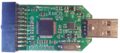
PCB, front
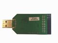
PCB, back


Protocol
TODO.