Difference between revisions of "Sysclk AX-Pro"
Jump to navigation
Jump to search
(→Hardware: + smt code) |
m |
||
| (5 intermediate revisions by 2 users not shown) | |||
| Line 4: | Line 4: | ||
| status = supported | | status = supported | ||
| source_code_dir = fx2lafw | | source_code_dir = fx2lafw | ||
| channels = 8 | | channels = 8 + 1 | ||
| samplerate = 8ch @ 24MHz, 8+1ch @ 12MHz | |||
| samplerate = 24MHz | |||
| samplerate_state = — | | samplerate_state = — | ||
| triggers = none (SW-only) | | triggers = none (SW-only) | ||
| Line 13: | Line 12: | ||
| memory = none | | memory = none | ||
| compression = none | | compression = none | ||
| price = $35 - $45 | |||
| website = [http://sysclk.taobao.com/ sysclk.taobao.com] | | website = [http://sysclk.taobao.com/ sysclk.taobao.com] | ||
}} | }} | ||
The '''Sysclk AX-Pro''' is a USB-based, 8-channel logic analyzer with up to 24MHz sampling rate, | The '''Sysclk AX-Pro''' is a USB-based, 8-channel logic analyzer with up to 24MHz sampling rate, with 1 additional analog channel (theoretically 2, but only one of them can be used at a time; 3MHz analog bandwidth). | ||
It is a clone of the [[CWAV USBee AX-Pro]]. | It is a clone of the [[CWAV USBee AX-Pro]]. | ||
| Line 22: | Line 22: | ||
In sigrok, we use the open-source [[fx2lafw]] firmware for this logic analyzer. | In sigrok, we use the open-source [[fx2lafw]] firmware for this logic analyzer. | ||
'''Note''': | '''Note''': [[fx2lafw]] currently doesn't support switching between the two possible analog channels, ACH2 will be used unconditionally. | ||
See [[Sysclk AX-Pro/Info]] for some more details (such as '''lsusb -v''' output) on the device. | See [[Sysclk AX-Pro/Info]] for some more details (such as '''lsusb -v''' output) on the device. | ||
| Line 39: | Line 39: | ||
* '''Analog channel switching relay''': TQ2-2V | * '''Analog channel switching relay''': TQ2-2V | ||
* '''Crystal''': 24MHz | * '''Crystal''': 24MHz | ||
The analog channels are multiplexed by relay or solid-state IC to one ADC. | The analog channels are multiplexed by relay or solid-state IC to one ADC. | ||
| Line 79: | Line 78: | ||
<gallery> | <gallery> | ||
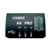
File:SysCLK_AX_Pro_box.jpg|<small> | File:SysCLK_AX_Pro_box.jpg|<small>Device, top</small> | ||
File:SysCLK_AX_Pro_top.jpg|<small>PCB, top</small> | File:SysCLK_AX_Pro_top.jpg|<small>PCB, top</small> | ||
File:SysCLK_AX_Pro_bottom.jpg|<small>PCB, bottom</small> | File:SysCLK_AX_Pro_bottom.jpg|<small>PCB, bottom</small> | ||
Latest revision as of 13:54, 30 June 2019
 | |
| Status | supported |
|---|---|
| Source code | fx2lafw |
| Channels | 8 + 1 |
| Samplerate | 8ch @ 24MHz, 8+1ch @ 12MHz |
| Samplerate (state) | — |
| Triggers | none (SW-only) |
| Min/max voltage |
Digital: -1V — +6V Analog: ±10V (±20V max) |
| Threshold voltage | Fixed: VIH=1.6V, VIL=1.4V |
| Memory | none |
| Compression | none |
| Price range | $35 - $45 |
| Website | sysclk.taobao.com |
The Sysclk AX-Pro is a USB-based, 8-channel logic analyzer with up to 24MHz sampling rate, with 1 additional analog channel (theoretically 2, but only one of them can be used at a time; 3MHz analog bandwidth).
It is a clone of the CWAV USBee AX-Pro.
In sigrok, we use the open-source fx2lafw firmware for this logic analyzer.
Note: fx2lafw currently doesn't support switching between the two possible analog channels, ACH2 will be used unconditionally.
See Sysclk AX-Pro/Info for some more details (such as lsusb -v output) on the device.
Hardware
- Main chip: Cypress CY7C68013A-56LTXC (FX2LP)
- I2C EEPROM: Atmel ATML125 24C02N SU27 D
- Auxiliary 8051 chip: STC STC15F104E (purpose is unknown)
- Supply voltage regulator: Advanced Monolithic Systems AMS1117-3.3
- Reference voltage regulator: Advanced Monolithic Systems AMS1117-2.851218
- Analog-to-Digital converter: Texas Instruments TLC5510I
- Analog input amplifiers: Analog Devices AD8065 (SMD marking "HRA")
- Analog amplifiers negative supply: Texas Instruments LMC7660
- Some operational amplifiers: Texas Instruments LM358
- Analog channel switching relay: TQ2-2V
- Crystal: 24MHz
The analog channels are multiplexed by relay or solid-state IC to one ADC.
FX2LP pin mappings
| # | Pin | Destination | Remark |
|---|---|---|---|
| 01 | RDY0/SLRD | TRIG | socket pin |
| 13 | IFCLK | GND | grounded |
| 18..25 | PB0..7 | DCH0..7 | digital input |
| 30 | CTL1/FLAGB | CLK | socket pin |
| 31 | CTL2/FLAGC | ADC_CLK | ADC clock input |
| 33 | PA0 | relay | multiplexing ACH1/ACH2 |
| 35 | PA2 | DCH1 GND | can be isolated from GND and act as aux socket pin |
| 36 | PA3 | DCH2 GND | can be isolated from GND and act as aux socket pin |
| 38 | PA5 | STC_P3.1 | aux 8051 chip |
| 39 | PA6 | STC_P3.3 | aux 8051 chip |
| 42 | RESET# | STC_P3.2 | aux 8051 chip |
| 44 | WAKEUP | NC | not connected |
| 45..52 | PD0..7 | ADC_D1..8 | ADC data output |
Photos
Protocol
Since we use the open-source fx2lafw firmware for this device, we don't need to know the protocol.


