Link Instruments MSO-19

The Link Instruments MSO-19 is a 2GSa/s (repetitive) or 200MSa/s (one-shot) one-channel oscilloscope, 200MSa/s eight-channel logic analyzer, 100MSa/s pattern generator and a TDR. Acquisition is done to local memory (1Ksa depth per channel) before samples get sent to the PC. It is small and USB powered, thus portable. Price is $249 (including probe, clips, wires and software). The MSO-28 specs are similar but this device provides two analog channels ($325).
See Link Instruments MSO-19/Info for more details (such as lsusb -vvv output) about the device.
Note: There is already some unused driver code in src/hardware/link-mso19 (see here).
Hardware
Photos
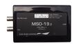
Device, front
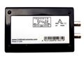
Device, back
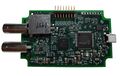
PCB, front
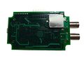
PCB, back


Protocol
USB protocol
It's just serial-over-USB, supported by the Linux kernel through the cp210x driver. The Link Instruments Vendor/Product ID (3195:f190) was added to the driver by kernel version 3.2.50. Earlier versions may need to be patched.
iSerial was exploited by Link Instruments to store hardware type, hardware revision, calibration quirks and the actual serial number.
- for an iSerial of 4294333650260000000 we have:
- 42943 336 502 6 0 000000
- vbit = 42943 / 10000
- dacoffset = 336
- offsetrange = 502
- hwmodel = 6
- hwrev = 0
- serial number = 000000
- 42943 336 502 6 0 000000
Serial protocol
- Control message
- Fixed header: 0x40, 0x4c, 0x44, 0x53, 0x7e
- Variable size payload, 16bit aligned
- Looks like each 16bits of payload are a register write operation
- register writes are 4bits for addr, 8 bits for value, 2 unused bits and 2 bits im not sure what they are for :)
- The simplest explanation for the unused bits is that the device bus width is 7 bits (being a CPLD that is very acceptable).
- The 2 special bits seem to be synchronization bits. 0x7e violates the conversion (high byte), and that may be used to reset the CPLD parser at the end of the packet.
- .?12 AAAA .?34 5678
- Conversion is: ((v & 0x3f) | ((v & 0xc0) << 6) | ((a & 0xf) << 8) | (((v ^ 0x20) & 0x20) << 1) | (((v ^ 0x80) & 0x80) << 7))
- Byte order is big endian
- Fixed footer: 0x7e
Registers description
There is no way to read from registers, only write is possible.
The purpose of registers 0 to 13 seems to depend on the value of the 2 lsbs of register 15.
Registers for ((R15 & 0x3) == 0x0):
- Read Sample buffer (1): Write 0 to this register to read the samples buffer.
- Read Trigger status (2): Write 0 to this register to read the trigger status.
- TRIGGER_CONFIG_L (3):
- lsbyte of the threshold value.
- TRIGGER_CONFIG_H (4):
- bits [1:0] hold the msbits of the threshold value
- (1 << 2): Trigger on falling edge
- (1 << 4 | 1 << 3): Select the purpose of the "Output" connector:
- 00 : Trigger pulse output
- 01 : PWM DAC from the pattern generator buffer.
- 10 : (?) never seen...
- 11 : White noise
- (1 << 6 | 1 << 5): These hold the DSO/LA trigger configuration:
- 00 : DSO level trigger
- 01 : DSO pulse trigger, width less than TRIGGER_WIDTH
- 10 : DSO pulse trigger, width equal or greater than TRIGGER_WIDTH
- 11 : LA combination trigger
- LA_TRIGGER(5): The value of the LA byte that generates a trigger event (in that mode).
- LA_TRIGGER_MASK(6): The mask for the LA_TRIGGER (bits set to 0 matter, those set to 1 are ignored).
- SCOPE_TRIGGER_HOLDOFF1 (7):
- SCOPE_TRIGGER_HOLDOFF2 (8): Store the trigger holdoff (delay between a triggering event and the trigger rearming).
- CLKRATE(9-10):
- TRIGGER_WIDTH (11): Stores the pulse width for the DSO pulse trigger, in sample units. Forced to be greater than 3 by the mso19 app.
- DAC(12-13):
Registers for ((R15 & 0x3) == 0x1):
This mode seems to be used to configure the pattern generator.
- REG_PATGEN_CLOCK1 (2) :
- REG_PATGEN_CLOCK2 (3) : Stores the sample clock configuration. Not sure how these two bytes work together...
- REG_PATGEN_START_L (4):
- REG_PATGEN_START_H (5): The start address for the pattern generator buffer (1023 samples long). When writing to the buffer, it is set to 0.
- REG_PATGEN_END_L (6):
- REG_PATGEN_END_H (7): The end address for the pattern generator buffer (1023 samples long). When writing the buffer, it is set to 0x3ff. When in normal mode (to set the end of the output) it is writen as the end address minus 2 (probably due to the actual implementation details).
- PATGEN_CFG (8): Configures the pattern generator.
- (1 << 0): Continuous mode ? (only seems to be allowed for the waveform generator, not for the pattern generator. why?)
- (1 << 1): Enter pattern write mode.
- (1 << 3 | 1 << 2):
- 11 : Manual start (starts after a pulse in PATGEN_TRIG)
- 10 : Start on MSO trigger
- 01 : Start on MSO "Go" (MSO trigger arm)
- 00 : Disabled
- PATGEN_TRIG (9): writen 0x1 and then 0x0, acts as a manual trigger to activate "stuff".
- PATGEN_WORD (10): In pattern write mode, takes the word for the current "instant".
- PATGEN_IO (11): In pattern write mode, writing 0x1 makes the instant an output one, and writing 0x0 makes it an input one (?)
- PATGEN_LOOPS (12): Stores the number of loops for the pattern generator. Set to 1 for pattern buffer writing mode.
- PATTERN_MASK (13): Stores the output bit mask (1 for enabled bits, 0 for disabled bits)
Registers for ((R15 & 0x3) == 0x2):
This mode is used to set the i2c or spi triggers.
NOTES:
- the difference between i2c and spi capture seems to be the TRIGGER_CFG_H bits (see R15 = 0)
- how does the hardware handle the start/stop conditions or the ack bit??
The protocol matcher seems to be comprised of a 4 byte shift register. The serial bits are shifted in through the last byte comparator (word 3) and exit through the first byte comparator (word 0). This is why if the trigger is set up with less than 3 words, the first bytes are the ones that end up matching everything (word set to 0x00, mask set to 0xff).
The mask bytes have their bits set to 1 for "ignore", and 0 for "match". The protocol matching block simply doing something this for every bit i:
matches[i] = (read[i] ^ word[i]) | mask[i]
The final result is the and'ing of the resulting 32 bits.
- TRIG_WORD0 (0): Hold the comparison words for the comparator.
- TRIG_WORD1 (1):
- TRIG_WORD2 (2):
- TRIG_WORD2 (3):
- TRIG_MASK0 (4): Holds the mask for the comparator (bits set at 1 always produce a positive match)
- TRIG_MASK1 (5):
- TRIG_MASK2 (6):
- TRIG_MASK3 (7):
- TRIG_SPI_MODE (8): Holds the SPI mode for triggering (valid modes 0, 1, 2, 3). Is set to 0 for I2C (not sure if mandatory)
Registers which don't seem to change purpose (so far):
- CONTROL1 (14):
- (1 << 0): Reset SFM
- (1 << 3): Force trigger
- (1 << 4): Enable ADC (?)
- (1 << 6): Reset ADC (?)
- (1 << 7): Led on/off
- CONTROL2 (15):
- (1 << 1 | 1 << 0): Control which register bank is selected for writing:
- 00: The DSO and LA control bank is selected
- 01: The PG (patern generator) control bank is selected
- 10: The PT (protocol trigger) control bank is selected
- (1 << 5): Slow mode (?) (set for the low clock rates, probably enables a clock divider)
- (1 << 1 | 1 << 0): Control which register bank is selected for writing:
Device reply description
- After writing 0x0 to the registers (1) or (2) of bank 0, the device replies with either 3072 bytes (1), or 1 byte (2).
- Only 7 bits are used from each byte.
- Bit (1 << 6) indicates which type of message this is:
- 0: This is a "status" message.
- 1: This is a "data" message.
STATUS ((1 << 6) == 0):
- The reply comprises just one byte. The lower nibble contains the trigger status (t), while the other two bits contain other status info (?)
- [ (ignored) 0 (h1) (h0) (t3) (t2) (t1) (t0) ]
Bit description:
- (1 << 5): Seems to be always set to 1 (?)
- (1 << 4): The state of the control bit (1 << 4): adc enabled (?).
- (1 << 3): Set to 1 upon successful triggering.
- (1 << 2): Set to 1 when the trigger block is armed and the adc (1 << 4) is also enabled (?)
- (1 << 1): Set to 1 when the trigger block is armed but the adc (1 << 4) is not (?)
- (1 << 0): Seems to be the oposite of bit (1 << 2) (?)
- Ususal values for t(3:0):
- 0x6: Triggered (data ready on the samples buffer).
- 0x4: Trigger armed
- 0x3: Someone messed up and armed the trigger without enabling ctl bit (1 << 4) (???)
- 0x1: Trigger not armed
DATA ((1 << 6) == 1):
- The reply is 24 bit aligned, and contains both the 10 bit analog sample data (a) and the 8 bit digital sample data (d).
- There's a total of 3072 bytes, comprising 1024 samples.
- For each group of 24 bits (a "sample"):
- (byte 0): [ (ignored) 1 (a5) (a4) (a3) (a2) (a1) (a0) ]
- (byte 1): [ (ignored) 1 (d1) (d0) (a9) (a8) (a7) (a6) ]
- (byte 2): [ (ignored) 1 (d7) (d6) (d5) (d4) (d3) (d2) ]
Device operation
The trigger status must be checked periodically, by writing 0 to the "Read Status" register (address 0 of bank 0). The returned value indicates the device status.
Startup:
- The MSO19 application starts by checking the device status. It accepts the values 0x21 or 0x31 as normal, before proceeding.
- It then resets the ADC, and checks for the device status again, and also accepts the values 0x21 and 0x31 as normal.
(...)
Capture Start:
Upon starting a capture, by hitting the "Go" button:
- If the DSO or the DAC need to be configured, the app resets the FSM (finite state machine), and then configures them both.
- If the PG needs to be configured, the app configures it.
- The app then arms the trigger system.
- Finally the app issues a trigger check (writing 0 to the register), and waits for the serial reply.
Handle Serial Reply:
- First the app checks how many bytes there are waiting on the serial port buffer. It only accepts two byte lengths, 3072 bytes and 1 byte.
- The app then checks if the first byte has bit 6 turned off ((byte & (1 << 6)) == 0), and if it is, it assumes it's a trigger status. Otherwise it assumes it's sample data.
Resources
- MSO-19 product page
- MSO-28 product page
- linkinstruments.com: PiMSO19
- GitHub: mso19fcgi (contains some source code for MSO-19)
- linkinstruments.com: PiMSO (for MSO-28)
- linkinstruments.com: MSO28 registers
- GitHub: mso28fcgi (contains some source code for MSO-28)