Difference between revisions of "Hantek PSO2020"
Jump to navigation
Jump to search
Uwe Hermann (talk | contribs) m (→EEPROM layout) |
(→Photos) |
||
| (8 intermediate revisions by 2 users not shown) | |||
| Line 22: | Line 22: | ||
* '''USB''': [http://www.cypress.com/documentation/datasheets/cy7c68013a-cy7c68014a-cy7c68015a-cy7c68016a-ez-usb-fx2lp-usb Cypress CY7C68013A-100AXC] (FX2LP) ([http://www.cypress.com/file/138911/download datasheet]) | * '''USB''': [http://www.cypress.com/documentation/datasheets/cy7c68013a-cy7c68014a-cy7c68015a-cy7c68016a-ez-usb-fx2lp-usb Cypress CY7C68013A-100AXC] (FX2LP) ([http://www.cypress.com/file/138911/download datasheet]) | ||
* '''256-byte I²C EEPROM''': [http://www.microchip.com/wwwproducts/en/24LC02B Microchip 24LC02BI] ([http://ww1.microchip.com/downloads/en/DeviceDoc/21709J.pdf datasheet]) | * '''256-byte I²C EEPROM''': [http://www.microchip.com/wwwproducts/en/24LC02B Microchip 24LC02BI] ([http://ww1.microchip.com/downloads/en/DeviceDoc/21709J.pdf datasheet]) | ||
* | * 1x '''8-channel analog multiplexer/demultiplexer''' (U6): [http://www.nexperia.com/products/logic/switches-multiplexers-de-multiplexers/digital-switches/74HC4051D.html NXP 74HC4051D] ([http://assets.nexperia.com/documents/data-sheet/74HC_HCT4051.pdf datasheet]) | ||
* '''1A low-dropout voltage regulator (3.3V):''' [http://www.advanced-monolithic.com/products/voltreg.html#1117 Advanced Monolithic Systems AMS1117-3.3] ([http://www.advanced-monolithic.com/pdf/ds1117.pdf datasheet]) | * '''1A low-dropout voltage regulator (3.3V):''' [http://www.advanced-monolithic.com/products/voltreg.html#1117 Advanced Monolithic Systems AMS1117-3.3] ([http://www.advanced-monolithic.com/pdf/ds1117.pdf datasheet]) | ||
* ?? '''2W, fixed input, isolated & unregulated dual/single output DC/DC converter''': [http://www.mornsun.cn/html/product/content/A_S-2WR2.html Mornsun A_S-2WR2 (A0505S-2WR2)] ([http://www.mornsun.cn/uploads/pdf/A_S-2WR2.pdf datasheet]) | * ?? '''2W, fixed input, isolated & unregulated dual/single output DC/DC converter''': [http://www.mornsun.cn/html/product/content/A_S-2WR2.html Mornsun A_S-2WR2 (A0505S-2WR2)] ([http://www.mornsun.cn/uploads/pdf/A_S-2WR2.pdf datasheet]) | ||
| Line 28: | Line 28: | ||
* ?? 4x '''145 MHz FastFET Op Amp''': [http://www.analog.com/en/products/amplifiers/operational-amplifiers/jfet-input-amplifiers/ad8065.html Analog Devices AD8065] ([http://www.analog.com/media/en/technical-documentation/data-sheets/AD8065-KGD-CHIP.pdf datasheet]) | * ?? 4x '''145 MHz FastFET Op Amp''': [http://www.analog.com/en/products/amplifiers/operational-amplifiers/jfet-input-amplifiers/ad8065.html Analog Devices AD8065] ([http://www.analog.com/media/en/technical-documentation/data-sheets/AD8065-KGD-CHIP.pdf datasheet]) | ||
* '''Crystal''': 24MHz | * '''Crystal''': 24MHz | ||
* 1x '''Photocoupler''' (U100): Toshiba TPL280 ([https://toshiba.semicon-storage.com/info/docget.jsp?did=16751&prodName=TLP280 datasheet]) | |||
* 1x '''4.5V Relay''' (used for High Voltage selection - U10): NEC UD2-4.5NU ([http://www.mouser.com/ds/2/212/KEM_R7005_UC2_UD2-541010.pdf datasheet]) | |||
* 1x '''±5V DC/DC Coverter''' (U13): INOUT A0505S ([https://www.mornsun-power.com/uploads/pdf/B_LS-1WR2.pdf datasheet]) | |||
| Line 52: | Line 55: | ||
|- | |- | ||
| S1, S2 | | S1, S2 | ||
| | | Tied to VCC. "Data Align Enabled (data from both channels available on rising edge of Clock A. Channel B data is delayed a 1/2 clock cycle).". | ||
|- | |- | ||
| DFS | | DFS | ||
| Tied to GND. Data format select = "offset binary" (not "twos complement"). | | Tied to GND. Data format select = "offset binary" (not "twos complement"). | ||
|- | |||
| REF_IN_A, REF_IN_B | |||
| Tied to REF_OUT. | |||
|- | |- | ||
| A<sub>IN</sub>A, A<sub>IN</sub>B | | A<sub>IN</sub>A, A<sub>IN</sub>B | ||
| Line 62: | Line 68: | ||
|} | |} | ||
'''Cypress FX2 pinout | '''Cypress FX2 pinout''': | ||
{| border="0" style="font-size: smaller" class="alternategrey sortable sigroktable" | {| border="0" style="font-size: smaller" class="alternategrey sortable sigroktable" | ||
|- | |- | ||
| Line 69: | Line 75: | ||
|- | |- | ||
| | | CTL0 | ||
| Connected to AD9288 ENC<sub>A</sub> | | Connected to AD9288 ENC<sub>A</sub>, to ENC<sub>B</sub> with an inverter. and to FX2 IFCLK. | ||
|- | |- | ||
| PB0-PB7 | | PB0-PB7 | ||
| Connected to AD9288 | | Connected to AD9288 D7<sub>A</sub>-D0<sub>A</sub>. '''Bit reversed!''' Must be reversed back in software. | ||
|- | |- | ||
| PD0-PD7 | | PD0-PD7 | ||
| Connected to AD9288 D0<sub>B</sub>-D7<sub>B</sub>. | | Connected to AD9288 D0<sub>B</sub>-D7<sub>B</sub>. | ||
|- | |||
| PA0, PA1, PA5 (Inputs) | |||
| Connected to the 3 buttons | |||
|- | |||
| PC0, PC3, PE?, PE? (Inputs) | |||
| Connected to the front selector | |||
|- | |||
| PC1 | |||
| Connected to S1 of the 74HC4051D mux | |||
|- | |||
| PC2 | |||
| Connected to S0 of the 74HC4051D mux | |||
|- | |||
| PC4 | |||
| AC/DC Selector | |||
|- | |- | ||
| PA7 | | PA7 | ||
| | | Voltage Selection Relay | ||
|- | |- | ||
| | | PA6 | ||
| Green LED | | Green LED | ||
|- | |||
| PE1 | |||
| Front light | |||
|- | |||
| PE2 | |||
| Red LED | |||
|} | |} | ||
| Line 96: | Line 121: | ||
File:Hantek_PSO2020_2.JPG|<small>Inside Back</small> | File:Hantek_PSO2020_2.JPG|<small>Inside Back</small> | ||
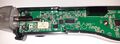
File:Hantek_PSO2020_3.JPG|<small>Inside Detail</small> | File:Hantek_PSO2020_3.JPG|<small>Inside Detail</small> | ||
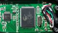
File:Pso2020_analog_input.jpg|<small>Analog input section</small> | |||
</gallery> | </gallery> | ||
Latest revision as of 22:41, 22 January 2024
 | |
| Status | |
|---|---|
| Source code | [1] |
| Channels | 1 |
| Samplerate | 96MHz |
| Analog bandwidth | 20MHz |
| Vertical resolution | 8bit |
| Triggers | none (SW-only) |
| Input impedance | 1MΩ‖25pF |
| Memory | none |
| Display | none |
| Connectivity | USB |
| Website | hantek.com |
The Hantek PSO2020 is a USB-based, 1-channel oscilloscope with an analog bandwidth of 20MS/s and 96MS/s sampling rate. Wide input rage, from ±100mV to ±50V.
See Hantek PSO2020/Info for more details (such as lsusb -v output) about the device.
Hardware
- USB: Cypress CY7C68013A-100AXC (FX2LP) (datasheet)
- 256-byte I²C EEPROM: Microchip 24LC02BI (datasheet)
- 1x 8-channel analog multiplexer/demultiplexer (U6): NXP 74HC4051D (datasheet)
- 1A low-dropout voltage regulator (3.3V): Advanced Monolithic Systems AMS1117-3.3 (datasheet)
- ?? 2W, fixed input, isolated & unregulated dual/single output DC/DC converter: Mornsun A_S-2WR2 (A0505S-2WR2) (datasheet)
- 8-bit, 40/80/100MHz, dual ADC: Analog Devices AD9288 (datasheet)
- ?? 4x 145 MHz FastFET Op Amp: Analog Devices AD8065 (datasheet)
- Crystal: 24MHz
- 1x Photocoupler (U100): Toshiba TPL280 (datasheet)
- 1x 4.5V Relay (used for High Voltage selection - U10): NEC UD2-4.5NU (datasheet)
- 1x ±5V DC/DC Coverter (U13): INOUT A0505S (datasheet)
Microchip 24LC02BI pinout:
| (Low, but not GND) A0 | 1- | O | -8 | VCC |
| (GND) A1 | 2- | -7 | WP (GND) | |
| (GND) A2 | 3- | -6 | SCL (FX2 SCL) | |
| VSS | 4- | -5 | SDA (FX2 SDA) |
Analog Devices ADS9288 pinout:
| AD9288 pins | Description |
|---|---|
| S1, S2 | Tied to VCC. "Data Align Enabled (data from both channels available on rising edge of Clock A. Channel B data is delayed a 1/2 clock cycle).". |
| DFS | Tied to GND. Data format select = "offset binary" (not "twos complement"). |
| REF_IN_A, REF_IN_B | Tied to REF_OUT. |
| AINA, AINB | Analog input channels. |
Cypress FX2 pinout:
| FX2 pins | Description |
|---|---|
| CTL0 | Connected to AD9288 ENCA, to ENCB with an inverter. and to FX2 IFCLK. |
| PB0-PB7 | Connected to AD9288 D7A-D0A. Bit reversed! Must be reversed back in software. |
| PD0-PD7 | Connected to AD9288 D0B-D7B. |
| PA0, PA1, PA5 (Inputs) | Connected to the 3 buttons |
| PC0, PC3, PE?, PE? (Inputs) | Connected to the front selector |
| PC1 | Connected to S1 of the 74HC4051D mux |
| PC2 | Connected to S0 of the 74HC4051D mux |
| PC4 | AC/DC Selector |
| PA7 | Voltage Selection Relay |
| PA6 | Green LED |
| PE1 | Front light |
| PE2 | Red LED |
Photos

Box Front

Box Back
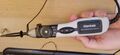
Device
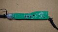
Inside Front
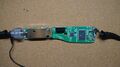
Inside Back
Inside Detail
Analog input section


Protocol
Firmware
Note: The firmware is not flashed into the device permanently! It will be automatically "uploaded" to the Cypress FX2's SRAM every time you attach the device to a USB port.
EEPROM layout
The device has a 256-byte I²C EEPROM with the following layout:
c0 b4 04 23 60 00 00 00 91 91 91 91 8a 8a 85 85
81 81 91 91 8a 8a 85 81 81 81 81 81 91 91 91 91
8a 8a 85 85 81 81 91 91 8a 8a 85 81 81 81 81 81
ff ff ff ff ff ff ff ff ff ff ff ff ff ff ff ff
ff ff ff ff ff ff ff ff ff ff ff ff ff ff ff ff
ff ff ff ff ff ff ff ff ff ff ff ff ff ff ff ff
ff ff ff ff ff ff ff ff ff ff ff ff ff ff ff ff
ff ff ff ff ff ff ff ff ff ff ff ff ff ff ff ff
ff ff ff ff ff ff ff ff ff ff ff ff ff ff ff ff
ff ff ff ff ff ff ff ff ff ff ff ff ff ff ff ff
ff ff ff ff ff ff ff ff ff ff ff ff ff ff ff ff
ff ff ff ff ff ff ff ff ff ff ff ff ff ff ff ff
ff ff ff ff ff ff ff ff ff ff ff ff ff ff ff ff
ff ff ff ff ff ff ff ff ff ff ff ff ff ff ff ff
ff ff ff ff ff ff ff ff ff ff ff ff ff ff ff ff
ff ff ff ff ff ff ff ff ff ff ff ff ff ff ff ff
Description:
| Bytes | Description |
|---|---|
| 0 | 0xc0: FX2 "c0 load" mode, i.e. VID/PID/DID are loaded from EEPROM (but not firmware). |
| 1-2 | 0x04b4: USB vendor ID (VID). |
| 3-4 | 0x6023: USB product ID (PID). |
| 5-6 | 0x0000: USB device ID (DID). |
| 7 | 0x00: FX2 configuration byte (see FX2 TRM for details). |
| 8-47 | Unknown. Possibly calibration data? |
| 48-255 | All-0xff. |