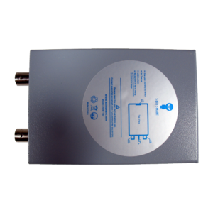
SainSmart DDS120
The SainSmart DDS120 is a USB-based, 2-channel oscilloscope with an analog bandwidth of 20MS/s and 48MS/s sampling rate.
See SainSmart DDS120/Info for more details (such as lsusb -v output) about the device.
- USB: Cypress CY7C68013A-100AXC (FX2LP) (datasheet)
- 256-byte I²C EEPROM: Microchip 24LC641 (datasheet)
- Crystal: 24MHz
- AD: AD8065ART-R2: (datasheet)
or in newer hardware
- AD: MXT2088 (datasheet)
- Opamp: Analog devices AD8065 (OPAMP)
- MUX: Texas Instruments CD4052B (2 x 1:4 MUX)
Firmware
The Sainsmart firmware is contained on an i2c eeprom. The FX2 boots directly into that firmware. Loading another firmware is possible but the os needs to support soft reset so it can reload the usb descriptors (linux does so via the USBDEVFS_RESET ioctl).
Vendor Protocol
| Oscilloscope command | bRequest value | Notes |
|---|---|---|
| Set CH0 coupling | 0x24 | Possible values: 0x00, 0x08 (AC-coupling, DC-coupling). |
| Set CH1 coupling | 0x25 | Possible values: 0x20, 0x10 (AC-coupling, DC-coupling). |
| Set CH0 voltage range | 0x22 | Possible values: 0x08, 0x04, 0x00, 0x06, 0x02 (50mV, 100mV, 200mV, 500mV, 1-5V). |
| Set CH1 voltage range | 0x23 | Possible values: 0x20, 0x10, 0x00, 0x12, 0x02 (50mV, 100mV, 200mV, 500mV, 1-5V). |
| Set sampling rate | 0x94 | Possible values: 0x11, 0x01, 0x10 (240kHz, 2.4MHz, 48MHz). |
| Trigger oscilloscope | 0x33 | Possible values: 0x00 == start sampling. |
Photos
Resources
Gain stage
The gain stage is 2 stage approach. -6dB and -20dB on the first stage (attentuator). The second stage is then doing the gain by 3 different resistor values switched into the feedback loop.
#Channel 0:
PC1=1; PC2=0; PC3= 0 -> Gain x0.1 = -20dB
PC1=1; PC2=0; PC3= 1 -> Gain x0.2 = -14dB
PC1=1; PC2=1; PC3= 0 -> Gain x0.4 =  -8dB
PC1=0; PC2=0; PC3= 0 -> Gain x0.5 =  -6dB
PC1=0; PC2=0; PC3= 1 -> Gain x1   =   0dB
PC1=0; PC2=1; PC3= 0 -> Gain x2   =  +6dB
#Channel 1:
PE1=1; PC4=0; PC5= 0 -> Gain x0.1 = -20dB
PE1=1; PC4=0; PC5= 1 -> Gain x0.2 = -14dB
PE1=1; PC4=1; PC5= 0 -> Gain x0.4 =  -8dB
PE1=0; PC4=0; PC5= 0 -> Gain x0.5 =  -6dB
PE1=0; PC4=0; PC5= 1 -> Gain x1   =   0dB
PE1=0; PC4=1; PC5= 0 -> Gain x2   =  +6dB
AC/DC coupling
The coupling is controlled via 2 PhotoMOS chips.
#Channel 0:
PE3=0 Disable AC-coupling capacitor (DC-Coupling)
PE3=1 Enable AC-coupling capacitor
#Channel 1:
PE0=0 Disable AC-coupling capacitor (DC-Coupling)
PE0=1 Enable AC-coupling capacitor
1kHz Calibration square wave
Pin PE2 controlls the level of the calibration output on the pcb. This is most likely driven by an ISR timer from the 8051 core of the FX2 chip.

