Difference between revisions of "XZL Studio DX"
m (add URL fragment to jump to page 48) |
|||
| (6 intermediate revisions by one other user not shown) | |||
| Line 1: | Line 1: | ||
{{DISPLAYTITLE:XZL_Studio DX}} | {{DISPLAYTITLE:XZL_Studio DX}} | ||
{{Infobox logic analyzer | {{Infobox logic analyzer | ||
| image = | | image = [[File:XZL Studio-DX front.jpg|180px]] | ||
| name = XZL_Studio DX | | name = XZL_Studio DX | ||
| status = | | status = supported | ||
| source_code_dir = fx2lafw | | source_code_dir = fx2lafw | ||
| channels = 16 + 2 | | channels = 16 + 2 | ||
| Line 21: | Line 21: | ||
See [[XZL_Studio DX/Info]] for some more details (such as '''lsusb -vvv''' output) on the device. | See [[XZL_Studio DX/Info]] for some more details (such as '''lsusb -vvv''' output) on the device. | ||
'''Note''':You need to chose one of "CWAV USBee DX" devices found in system ( ''sigrok-ok --scan'' ). One of them is digital (supported, 16 channels). Other show 16 digital channels too, but it is for 2x analog input and not working yet. | |||
'''Note''': Due to the fact that this device has two FX2 chips behind a USB hub inside, this will need extra code to enumerate correctly in sigrok. Do you have this device? Let us know! | '''Note''': Due to the fact that this device has two FX2 chips behind a USB hub inside, this will need extra code to enumerate correctly in sigrok. Do you have this device? Let us know! | ||
'''Note''': Idea how sync 2 chips works. Second FX2 is responsible for reading ADC data only, but it can't initialise processing. It can only get info from first chip that he need to read data -> pin SLWR. So it means that if second chip do conversions only when triggered, then there are exactly that same number of samples read from both chips, from that same time... Look at 48 page of [http://www.cypress.com/?docID=45142#page=48 Cypress CY7C68013A-56LTXC (FX2LP)] "Slave FIFO Asynchronous Write" | |||
== Hardware == | == Hardware == | ||
| Line 28: | Line 32: | ||
* '''Main chip''': 2x [http://www.cypress.com/?docID=45142 Cypress CY7C68013A-56LTXC (FX2LP)] | * '''Main chip''': 2x [http://www.cypress.com/?docID=45142 Cypress CY7C68013A-56LTXC (FX2LP)] | ||
* '''Analog-to-Digital converter''': 2x [http://www.ti.com/lit/ds/symlink/tlc5510.pdf Texas Instruments TLC5510I (SO 24pin package)] | * '''Analog-to-Digital converter''': 2x [http://www.ti.com/lit/ds/symlink/tlc5510.pdf Texas Instruments TLC5510I (SO 24pin package)] | ||
* '''I2C EEPROM''': | * '''I2C EEPROM''': ATMLH136 24C02C M Y, place for second EEPROM chip [http://ww1.microchip.com/downloads/en/DeviceDoc/21202J.pdf reference]. | ||
* '''USB 2.0 Hub''': SMSC USB2512A (QFN 36-pin package) | * '''USB 2.0 Hub''': [http://www.mouser.com/catalog/specsheets/2512adb.pdf SMSC USB2512A (QFN 36-pin package)] | ||
* '''Low-dropout voltage regulator''': Advanced Monolithic Systems AMS1117-3.3 | * '''Low-dropout voltage regulator''': [http://www.advanced-monolithic.com/pdf/ds1117.pdf Advanced Monolithic Systems AMS1117-3.3] | ||
* '''CMOS Voltage Converter''': 2x 7660 AIBAZ V01828A | * '''CMOS Voltage Converter''': 2x [https://www.ti.com/lit/ds/symlink/lmc7660.pdf 7660 AIBAZ V01828A] | ||
* '''Crystal''': 24MHz | * '''Crystal''': 24MHz | ||
* ... | * ... | ||
| Line 37: | Line 41: | ||
Two jumpers: | Two jumpers: | ||
* '''P1''' jumper - WRITE PROTECT, Connects WP EEPROM pin [7] to Vcc. If pin is closed, Write Protection is enabled. | * '''P1''' jumper - WRITE PROTECT, Connects WP EEPROM pin [7] to Vcc. If pin is closed, Write Protection is enabled. | ||
* '''P3''' jumper - EEPROM CONNECTION, connects SDA EEPROM pin [5] to | * '''P3''' jumper - EEPROM CONNECTION, connects SDA EEPROM pin [5] to SDA pins on both CY7C68013A (if open there is no connection) | ||
Extra info,<br/> | Extra info,<br/> | ||
It looks that place for second eeprom is designed as backup memory. If P4 is closed, and P3 is open, then only spare memory is connected. | It looks that place for second eeprom is designed as backup memory. If P4 is closed, and P3 is open, then only spare memory is connected. | ||
== Pin mapping == | |||
Needed for use (I don't know how to remap pins yet) | |||
Current PIN meaning - instead of that what is printed on device (for sigrok 0.8) | |||
{| border="0" style="font-size: smaller;" class="alternategrey sigroktable" | |||
|- | |||
| 4 || 15 | |||
|- | |||
| 5 || 14 | |||
|- | |||
| 6 || 13 | |||
|- | |||
| 7 || 8 | |||
|- | |||
| 3 || 9 | |||
|- | |||
| 2 || 10 | |||
|- | |||
| 1 || 11 | |||
|- | |||
| 0 || 12 | |||
|- | |||
| TRIG || GND | |||
|- | |||
| 5V || GND | |||
|- | |||
|} | |||
== | === First FX2LP pin mappings === | ||
Responsible for all digital inputs (0-15) and TRIG. Now it works with latest software version, but channels numbers are scrambled: | |||
Responsible for all digital inputs (0-15). Now it works with latest software version, but channels are scrambled: | |||
{| border="0" style="font-size: smaller;" class="alternategrey sigroktable" | {| border="0" style="font-size: smaller;" class="alternategrey sigroktable" | ||
| Line 85: | Line 117: | ||
|- | |- | ||
| 36 || CTL0/FLAGA || TRIG || socket pin | | 36 || CTL0/FLAGA || TRIG || socket pin | ||
|- | |||
| 37 || CTL1/*FLAGB || ADC [1,2] CLK + RDY1/SLWR on second FX2LP || signal for both ADC and secondary FX2 | |||
|- | |- | ||
| 21 || Reserved || GND || | | 21 || Reserved || GND || | ||
| Line 91: | Line 125: | ||
Second | === Second FX2LP pin mappings === | ||
Connected to both ADCs <br/> | Connected to both ADCs <br/> | ||
| Line 100: | Line 134: | ||
! # !! Pin !! Destination !! Remark | ! # !! Pin !! Destination !! Remark | ||
|- | |- | ||
| 9 || RDY1/SLWR || ADC [1,2] CLK || ADC_clock, | | 9 || RDY1/SLWR || CL1 on first FXLP and ADC [1,2] CLK || input: ADC_clock, signal to start read data | ||
|- | |- | ||
| 25-32 || FD0-FD7 || ADC CH1, D1-D8 || ADC_data for channel 1 | | 25-32 || FD0-FD7 || ADC CH1, D1-D8 || ADC_data for channel 1 | ||
| Line 111: | Line 145: | ||
|} | |} | ||
TODO - check rest of the pins | ''TODO'' - check rest of the pins | ||
EEPROM - connected to both (!) CY7C68013A processors <br/> | EEPROM - connected to both (!) CY7C68013A processors <br/> | ||
| Line 124: | Line 158: | ||
|- | |- | ||
|} | |} | ||
== Photos == | == Photos == | ||
| Line 150: | Line 182: | ||
[[Category:Oscilloscope]] | [[Category:Oscilloscope]] | ||
[[Category:Mixed-signal oscilloscope]] | [[Category:Mixed-signal oscilloscope]] | ||
[[Category: | [[Category:Supported]] | ||
[[Category:In progress]] | |||
Revision as of 01:11, 11 March 2018
 | |
| Status | supported |
|---|---|
| Source code | fx2lafw |
| Channels | 16 + 2 |
| Samplerate | 24MHz |
| Samplerate (state) | — |
| Triggers | none (SW-only) |
| Min/max voltage |
Digital 0 — 5.4V Analog ±10V |
| Threshold voltage | Fixed: VIH=1.4V, VIL=0.8V |
| Memory | none |
| Compression | none |
| Website | hotmcu.com |
The XZL_Studio DX is a USB-based, 16-channel logic analyzer with up to 24MHz sampling rate, and with 2 additional analog channels.
It is a clone of the CWAV USBee DX.
See XZL_Studio DX/Info for some more details (such as lsusb -vvv output) on the device.
Note:You need to chose one of "CWAV USBee DX" devices found in system ( sigrok-ok --scan ). One of them is digital (supported, 16 channels). Other show 16 digital channels too, but it is for 2x analog input and not working yet.
Note: Due to the fact that this device has two FX2 chips behind a USB hub inside, this will need extra code to enumerate correctly in sigrok. Do you have this device? Let us know!
Note: Idea how sync 2 chips works. Second FX2 is responsible for reading ADC data only, but it can't initialise processing. It can only get info from first chip that he need to read data -> pin SLWR. So it means that if second chip do conversions only when triggered, then there are exactly that same number of samples read from both chips, from that same time... Look at 48 page of Cypress CY7C68013A-56LTXC (FX2LP) "Slave FIFO Asynchronous Write"
Hardware
- Main chip: 2x Cypress CY7C68013A-56LTXC (FX2LP)
- Analog-to-Digital converter: 2x Texas Instruments TLC5510I (SO 24pin package)
- I2C EEPROM: ATMLH136 24C02C M Y, place for second EEPROM chip reference.
- USB 2.0 Hub: SMSC USB2512A (QFN 36-pin package)
- Low-dropout voltage regulator: Advanced Monolithic Systems AMS1117-3.3
- CMOS Voltage Converter: 2x 7660 AIBAZ V01828A
- Crystal: 24MHz
- ...
Two jumpers:
- P1 jumper - WRITE PROTECT, Connects WP EEPROM pin [7] to Vcc. If pin is closed, Write Protection is enabled.
- P3 jumper - EEPROM CONNECTION, connects SDA EEPROM pin [5] to SDA pins on both CY7C68013A (if open there is no connection)
Extra info,
It looks that place for second eeprom is designed as backup memory. If P4 is closed, and P3 is open, then only spare memory is connected.
Pin mapping
Needed for use (I don't know how to remap pins yet)
Current PIN meaning - instead of that what is printed on device (for sigrok 0.8)
| 4 | 15 |
| 5 | 14 |
| 6 | 13 |
| 7 | 8 |
| 3 | 9 |
| 2 | 10 |
| 1 | 11 |
| 0 | 12 |
| TRIG | GND |
| 5V | GND |
First FX2LP pin mappings
Responsible for all digital inputs (0-15) and TRIG. Now it works with latest software version, but channels numbers are scrambled:
| # | Pin | Destination | Remark |
|---|---|---|---|
| FD4 | 0 | digital input | |
| FD5 | 1 | digital input | |
| FD6 | 2 | digital input | |
| FD7 | 3 | digital input | |
| FD3 | 4 | digital input | |
| FD2 | 5 | digital input | |
| FD1 | 6 | digital input | |
| FD0 | 7 | digital input | |
| FD15 | 8 | digital input | |
| FD14 | 9 | digital input | |
| FD13 | a | digital input | |
| FD8 | b | digital input | |
| FD9 | c | digital input | |
| FD10 | d | digital input | |
| FD11 | e | digital input | |
| FD12 | f | digital input | |
| 36 | CTL0/FLAGA | TRIG | socket pin |
| 37 | CTL1/*FLAGB | ADC [1,2] CLK + RDY1/SLWR on second FX2LP | signal for both ADC and secondary FX2 |
| 21 | Reserved | GND |
Second FX2LP pin mappings
Connected to both ADCs
FX2LP pin mappings
| # | Pin | Destination | Remark |
|---|---|---|---|
| 9 | RDY1/SLWR | CL1 on first FXLP and ADC [1,2] CLK | input: ADC_clock, signal to start read data |
| 25-32 | FD0-FD7 | ADC CH1, D1-D8 | ADC_data for channel 1 |
| 42-56,1-3 | FD8-FD15 | ADC CH2, D1-D8 | ADC_data for channel 2 |
| 45 | PA5/FIFOADR1 | GND | gnd ? to check |
| 47 | PA7/*FLAGD/SLCS# | GND | gnd ? to check? probably can be used do distinguish chips |
TODO - check rest of the pins
EEPROM - connected to both (!) CY7C68013A processors
| # | EEPROM | Processor | |
|---|---|---|---|
| SDA | SDA | via jumper | |
| SCL | SCL |
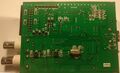
Photos
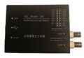
Device, top
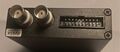
Device, connectors
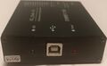
Device, usb
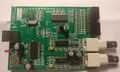
PCB, top
PCB, bottom


Protocol
Since we use the open-source fx2lafw firmware for this device, we don't need to know the protocol.
Resources
TODO.