Difference between revisions of "XZL Studio DX"
| (3 intermediate revisions by the same user not shown) | |||
| Line 45: | Line 45: | ||
== Pin mapping == | == Pin mapping == | ||
First CY7C68013A <br/> | '''First CY7C68013A''' <br/> | ||
Responsible for all digital inputs (0-15). Now it works with latest software version, but channels are | Responsible for all digital inputs (0-15). Now it works with latest software version, but channels are scrambled: | ||
{| border="0" style="font-size: smaller;" class="alternategrey sigroktable" | {| border="0" style="font-size: smaller;" class="alternategrey sigroktable" | ||
|- | |- | ||
! # !! | ! # !! Pin !! Destination !! Remark | ||
|- | |- | ||
| || 0 || | | || FD4 || 0 || digital input | ||
|- | |- | ||
| || 1 || | | || FD5 || 1 || digital input | ||
|- | |- | ||
| || 2 || | | || FD6 || 2 || digital input | ||
|- | |- | ||
| || 3 || | | || FD7 || 3 || digital input | ||
|- | |- | ||
| || 4 || | | || FD3 || 4 || digital input | ||
|- | |- | ||
| || 5 || | | || FD2 || 5 || digital input | ||
|- | |- | ||
| || 6 || | | || FD1 || 6 || digital input | ||
|- | |- | ||
| || 7 || | | || FD0 || 7 || digital input | ||
|- | |- | ||
| || 8 || | | || FD15 || 8 || digital input | ||
|- | |- | ||
| || 9 || | | || FD14 || 9 || digital input | ||
|- | |- | ||
| || a || | | || FD13 || a || digital input | ||
|- | |- | ||
| || b || | | || FD8 || b || digital input | ||
|- | |- | ||
| || c || | | || FD9 || c || digital input | ||
|- | |- | ||
| || d || | | || FD10 || d || digital input | ||
|- | |- | ||
| || e || | | || FD11 || e || digital input | ||
|- | |- | ||
| || f || | | || FD12 || f || digital input | ||
|- | |||
| 36 || CTL0/FLAGA || TRIG || socket pin | |||
|- | |||
| 21 || Reserved || GND || | |||
|- | |- | ||
|} | |} | ||
| Line 89: | Line 93: | ||
Second CY7C68013A <br/> | Second CY7C68013A <br/> | ||
Connected to both ADCs | Connected to both ADCs <br/> | ||
FX2LP pin mappings <br/> | |||
{| border="0" style="font-size: smaller;" class="alternategrey sigroktable" | |||
|- | |||
! # !! Pin !! Desitination for CH1 !! Desitination for CH2 !! Remark | |||
|- | |||
| || CLS || RDY1/SLWR || RDY1/SLWR || ADC_clock, both ADC connected to single pin | |||
|- | |||
| || D1-D8 || FD0-FD7 || FD8-DF15 || ADC_data | |||
|- | |||
| 45 || 45 PA5/FIFOADR1 || GND || GND || gnd ? to check | |||
|- | |||
| 47 || PA7/*FLAGD/SLCS# || GND || GND || gnd ? to check? probably can be used do distinguish chips | |||
|} | |||
TODO - check rest of the pins | |||
EEPROM - connected to both (!) CY7C68013A processors <br/> | |||
{| border="0" style="font-size: smaller;" class="alternategrey sigroktable" | |||
|- | |||
! # !! EEPROM !! Processor !! | |||
|- | |||
| || SDA || SDA || via jumper | |||
|- | |||
| || SCL || SCL || | |||
|- | |||
|} | |||
TODO | TODO | ||
Revision as of 23:51, 8 March 2018
| Status | planned |
|---|---|
| Source code | fx2lafw |
| Channels | 16 + 2 |
| Samplerate | 24MHz |
| Samplerate (state) | — |
| Triggers | none (SW-only) |
| Min/max voltage |
Digital 0 — 5.4V Analog ±10V |
| Threshold voltage | Fixed: VIH=1.4V, VIL=0.8V |
| Memory | none |
| Compression | none |
| Website | hotmcu.com |
The XZL_Studio DX is a USB-based, 16-channel logic analyzer with up to 24MHz sampling rate, and with 2 additional analog channels.
It is a clone of the CWAV USBee DX.
See XZL_Studio DX/Info for some more details (such as lsusb -vvv output) on the device.
Note: Due to the fact that this device has two FX2 chips behind a USB hub inside, this will need extra code to enumerate correctly in sigrok. Do you have this device? Let us know!
Hardware
- Main chip: 2x Cypress CY7C68013A-56LTXC (FX2LP)
- Analog-to-Digital converter: 2x Texas Instruments TLC5510I (SO 24pin package)
- I2C EEPROM: Atmel ATML H136 24C02C M Y, place for second EEPROM chip.
- USB 2.0 Hub: SMSC USB2512A (QFN 36-pin package)
- Low-dropout voltage regulator: Advanced Monolithic Systems AMS1117-3.3
- CMOS Voltage Converter: 2x 7660 AIBAZ V01828A
- Crystal: 24MHz
- ...
Two jumpers:
- P1 jumper - WRITE PROTECT, Connects WP EEPROM pin [7] to Vcc. If pin is closed, Write Protection is enabled.
- P3 jumper - EEPROM CONNECTION, connects SDA EEPROM pin [5] to some pin on second CY7C68013A (if open there is no connection)
Extra info,
It looks that place for second eeprom is designed as backup memory. If P4 is closed, and P3 is open, then only spare memory is connected.
Pin mapping
First CY7C68013A
Responsible for all digital inputs (0-15). Now it works with latest software version, but channels are scrambled:
| # | Pin | Destination | Remark |
|---|---|---|---|
| FD4 | 0 | digital input | |
| FD5 | 1 | digital input | |
| FD6 | 2 | digital input | |
| FD7 | 3 | digital input | |
| FD3 | 4 | digital input | |
| FD2 | 5 | digital input | |
| FD1 | 6 | digital input | |
| FD0 | 7 | digital input | |
| FD15 | 8 | digital input | |
| FD14 | 9 | digital input | |
| FD13 | a | digital input | |
| FD8 | b | digital input | |
| FD9 | c | digital input | |
| FD10 | d | digital input | |
| FD11 | e | digital input | |
| FD12 | f | digital input | |
| 36 | CTL0/FLAGA | TRIG | socket pin |
| 21 | Reserved | GND |
Second CY7C68013A
Connected to both ADCs
FX2LP pin mappings
| # | Pin | Desitination for CH1 | Desitination for CH2 | Remark |
|---|---|---|---|---|
| CLS | RDY1/SLWR | RDY1/SLWR | ADC_clock, both ADC connected to single pin | |
| D1-D8 | FD0-FD7 | FD8-DF15 | ADC_data | |
| 45 | 45 PA5/FIFOADR1 | GND | GND | gnd ? to check |
| 47 | PA7/*FLAGD/SLCS# | GND | GND | gnd ? to check? probably can be used do distinguish chips |
TODO - check rest of the pins
EEPROM - connected to both (!) CY7C68013A processors
| # | EEPROM | Processor | |
|---|---|---|---|
| SDA | SDA | via jumper | |
| SCL | SCL |
TODO
Photos
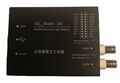
Device, top
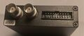
Device, connectors
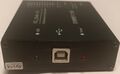
Device, usb
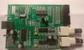
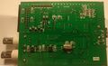
PCB, top
PCB, bottom


Protocol
Since we use the open-source fx2lafw firmware for this device, we don't need to know the protocol.
Resources
TODO.