Difference between revisions of "Sysclk LWLA1034"
Jump to navigation
Jump to search
(Change status to "In progress") |
Uwe Hermann (talk | contribs) m |
||
| Line 1: | Line 1: | ||
[[File:Sysclk lwla1034.jpg| | {{Infobox logic analyzer | ||
| image = [[File:Sysclk lwla1034.jpg|180px]] | |||
| name = Sysclk LWLA1034 | |||
| status = in progress | |||
| source_code_dir = | |||
| channels = 34 | |||
| samplerate = 125MHz | |||
| samplerate_state = ? | |||
| triggers = ? | |||
| voltages = ? | |||
| threshold = ? | |||
| memory = 256Kbit/channel | |||
| compression = ? | |||
| website = [http://item.taobao.com/item.htm?id=19834430293 taobao.com] | |||
}} | |||
The | The '''Sysclk LWLA1034''' is a USB-based, 34-channel logic analyzer with up to 125MHz sampling rate. | ||
See [[Sysclk LWLA1034/Info]] for more details (such as '''lsusb - | See [[Sysclk LWLA1034/Info]] for more details (such as '''lsusb -v''' output) about the device. | ||
== Hardware == | == Hardware == | ||
* Altera EP2C5Q208C8N (Cyclone II) FPGA | * Altera EP2C5Q208C8N (Cyclone II) FPGA | ||
* Cypress CY7C68013A-56 (FX2) USB interface chip | * Cypress CY7C68013A-56 (FX2) USB interface chip | ||
| Line 13: | Line 28: | ||
<gallery> | <gallery> | ||
File:Sysclk lwla1034 pcb top.jpg|PCB top | File:Sysclk lwla1034 pcb top.jpg|<small>PCB, top</small> | ||
File:Sysclk lwla1034 pcb bottom.jpg|PCB bottom | File:Sysclk lwla1034 pcb bottom.jpg|<small>PCB, bottom</small> | ||
File:Sysclk lwla1034 pcb closeup.jpg|PCB close-up | File:Sysclk lwla1034 pcb closeup.jpg|<small>PCB, close-up</small> | ||
File:Sysclk lwla1034 chip2.jpg|FX2 | File:Sysclk lwla1034 chip2.jpg|<small>Cypress FX2</small> | ||
File:Sysclk lwla1034 chip3 removed marking.jpg|SRAM (marking removed) | File:Sysclk lwla1034 chip3 removed marking.jpg|<small>SRAM (marking removed)</small> | ||
</gallery> | </gallery> | ||
| Line 29: | Line 44: | ||
* The FX2 firmware appears to be loaded from an EEPROM on the board, so that the final USB device descriptor is immediately available on power-up. | * The FX2 firmware appears to be loaded from an EEPROM on the board, so that the final USB device descriptor is immediately available on power-up. | ||
* | * Endpoint 4 appears to be used exclusively for loading a new bitstream into the FPGA. | ||
* | * Endpoint 2 is apparently used for sending commands to the FPGA firmware, with responses (if any) coming in from endpoint 6. | ||
Reverse engineering of the vendor protocol is currently in progress. See [[Sysclk LWLA1034/Protocol]] for a documentation of the findings gathered so far. | Reverse engineering of the vendor protocol is currently in progress. See [[Sysclk LWLA1034/Protocol]] for a documentation of the findings gathered so far. | ||
| Line 36: | Line 51: | ||
== Resources == | == Resources == | ||
[http://blog.csdn.net/mcupro | * [http://blog.csdn.net/mcupro Mcupro blog on CSDN] | ||
[[Category:Device]] | [[Category:Device]] | ||
[[Category:Logic analyzer]] | [[Category:Logic analyzer]] | ||
[[Category:In progress]] | [[Category:In progress]] | ||
Revision as of 22:13, 4 January 2014
 | |
| Status | in progress |
|---|---|
| Channels | 34 |
| Samplerate | 125MHz |
| Samplerate (state) | ? |
| Triggers | ? |
| Min/max voltage | ? |
| Threshold voltage | ? |
| Memory | 256Kbit/channel |
| Compression | ? |
| Website | taobao.com |
The Sysclk LWLA1034 is a USB-based, 34-channel logic analyzer with up to 125MHz sampling rate.
See Sysclk LWLA1034/Info for more details (such as lsusb -v output) about the device.
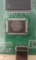
Hardware
- Altera EP2C5Q208C8N (Cyclone II) FPGA
- Cypress CY7C68013A-56 (FX2) USB interface chip
- Cypress 256k×36 SRAM (likely a CY7C1361C-133AXC or similar)
Photos
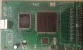
PCB, top
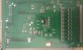
PCB, bottom
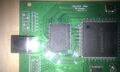
PCB, close-up
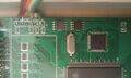
Cypress FX2
SRAM (marking removed)


The not-installed 10-pin connector between the USB socket and the large capacitor seems to connect to the JTAG pins of the FPGA.
Software

Firmware
- The FX2 firmware appears to be loaded from an EEPROM on the board, so that the final USB device descriptor is immediately available on power-up.
- Endpoint 4 appears to be used exclusively for loading a new bitstream into the FPGA.
- Endpoint 2 is apparently used for sending commands to the FPGA firmware, with responses (if any) coming in from endpoint 6.
Reverse engineering of the vendor protocol is currently in progress. See Sysclk LWLA1034/Protocol for a documentation of the findings gathered so far.