Difference between revisions of "Saleae Logic16"
Uwe Hermann (talk | contribs) m (→Hardware) |
m (→Hardware: updated C7C68013A datasheet URL) |
||
| (22 intermediate revisions by 5 users not shown) | |||
| Line 1: | Line 1: | ||
{{Infobox logic analyzer | {{Infobox logic analyzer | ||
| image = [[File:Saleae Logic16. | | image = [[File:Saleae Logic16 bottom.png|180px]] | ||
| name = Saleae Logic16 | | name = Saleae Logic16 | ||
| status = | | status = supported | ||
| source_code_dir = | | source_code_dir = saleae-logic16 | ||
| channels = | | channels = 3/6/9/16 | ||
| samplerate = 100/50/ | | samplerate = 100/50/32/16MHz | ||
| samplerate_state = — | | samplerate_state = — | ||
| triggers = none (SW-only) | | triggers = none (SW-only) | ||
| voltages = -0.9V — 6V | | voltages = -0.9V — 6V | ||
| threshold = configurable:<br />for 1.8V to 3.6V systems: | | threshold = configurable:<br />for 1.8V to 3.6V systems: V<sub>IH</sub>=1.4V, V<sub>IL</sub>=0.7V<br />for 5V systems: V<sub>IH</sub>=3.6V, V<sub>IL</sub>=1.4V | ||
| memory = none | | memory = none | ||
| compression = yes | | compression = yes | ||
| Line 15: | Line 15: | ||
}} | }} | ||
The '''Saleae Logic16''' is a USB-based, 16-channel logic analyzer with 100/50/ | The '''Saleae Logic16''' is a USB-based, 16-channel logic analyzer with 100/50/32/16MHz sampling rate (at 3/6/9/16 enabled channels). | ||
The case requires a '''Torx T5''' screwdriver to open. | The case requires a '''Torx T5''' screwdriver to open. | ||
See [[Saleae Logic16/Info]] for more details (such as '''lsusb - | See [[Saleae Logic16/Info]] for more details (such as '''lsusb -v''' output) about the device. | ||
See [[Saleae Logic]] for the predecessor product of the Saleae Logic16. | See [[Saleae Logic]] for the predecessor product of the Saleae Logic16. | ||
| Line 26: | Line 26: | ||
* '''FPGA''': [http://www.xilinx.com/support/index.html/content/xilinx/en/supportNav/silicon_devices/fpga/spartan-3a.html Xilinx Spartan-3A XC3S200A], 200K gates ([http://www.xilinx.com/support/documentation/data_sheets/ds529.pdf datasheeet]) | * '''FPGA''': [http://www.xilinx.com/support/index.html/content/xilinx/en/supportNav/silicon_devices/fpga/spartan-3a.html Xilinx Spartan-3A XC3S200A], 200K gates ([http://www.xilinx.com/support/documentation/data_sheets/ds529.pdf datasheeet]) | ||
* '''USB interface chip''': [http://www.cypress.com/?mpn=CY7C68013A-56PVXC Cypress CY7C68013A-56PVXC (FX2LP)] ([http://www.cypress.com/ | * '''USB interface chip''': [http://www.cypress.com/?mpn=CY7C68013A-56PVXC Cypress CY7C68013A-56PVXC (FX2LP)] ([http://www.cypress.com/file/138911/download datasheet]) | ||
* '''Ultralow capacitance ESD protection''': 4x [http://www.st.com/web/catalog/sense_power/FM114/CL1137/SC1490/PF109008 ST DVIULC6-4SC6] ([http://www.st.com/st-web-ui/static/active/en/resource/technical/document/datasheet/CD00065974.pdf datasheet]) | * '''Ultralow capacitance ESD protection''': 4x [http://www.st.com/web/catalog/sense_power/FM114/CL1137/SC1490/PF109008 ST DVIULC6-4SC6] ([http://www.st.com/st-web-ui/static/active/en/resource/technical/document/datasheet/CD00065974.pdf datasheet]) | ||
* '''I2C EEPROM''': | * '''2Kbit I2C EEPROM''': [http://www.microchip.com/wwwproducts/Devices.aspx?dDocName=en010774 Microchip 24AA02] ([http://ww1.microchip.com/downloads/en/DeviceDoc/21709J.pdf datasheet]) (marking: "B2TH", starts with "B2" always, the last 2 characters are a "traceability code") | ||
* ''' | * '''2.5MHz, 1.5A synchronous step down switching regulator (1.2V)''': [http://www.semtech.com/power-management/switching-regulators/sc189 Semtech SC189] ([http://www.semtech.com/images/datasheet/sc189.pdf datasheet]) (marking: "189C") | ||
* ''' | * '''2.5MHz, 1.5A synchronous step down switching regulator (3.3V)''': [http://www.semtech.com/power-management/switching-regulators/sc189 Semtech SC189] ([http://www.semtech.com/images/datasheet/sc189.pdf datasheet]) (marking: "189Z") | ||
* '''N-MOSFET''': 2x 2N7002 type MOSFET (marking: "72Y7"). Connected as "low-side" switch/LED driver and inverter. | |||
'''Pinouts and connections:''' | '''Pinouts and connections:''' | ||
| Line 36: | Line 37: | ||
'''JTAG header (FPGA):''' | '''JTAG header (FPGA):''' | ||
The '''J3''' pin header is a JTAG connector wired to the FPGA. The pins are (from left to right, the right-most pin is square): | The '''J3''' pin header is a JTAG connector wired to the FPGA. The pins are (from left to right, the right-most pin, pin number 1, is square): | ||
{| border="0" style="font-size: smaller" class="sigroktable" | {| border="0" style="font-size: smaller" class="sigroktable" | ||
|- | |- | ||
!5 | |||
!4 | |||
!3 | |||
!2 | |||
!1 | !1 | ||
|- | |- | ||
| Line 71: | Line 72: | ||
'''Cypress FX2:''' | '''Cypress FX2:''' | ||
<small> | |||
{{chip_56pin | |||
| 1=<span style="color:green">(FPGA 15, IO_L05P_3)</span> PD5 | |||
| 2=<span style="color:green">(FPGA 13, IO_L04N_3)</span> PD6 | |||
| 3=<span style="color:green">(FPGA 10, IO_L03N_3)</span> PD7 | |||
| 4=GND | |||
| 5=<span style="color:green">(FPGA 90, IO_0)</span> CLKOUT | |||
| 6=VCC | |||
| 7=GND | |||
| 8=<span style="color:green">(FPGA 3, IO_L01P_3)</span> RDY0/*SLRD | |||
| 9=<span style="color:green">(FPGA 16, IO_L05N_3)</span> RDY1/*SLWR | |||
| 10=AVCC | |||
| 11=<span style="color:brown">(24MHz crystal)</span> XTALOUT | |||
| 12=<span style="color:brown">(24MHz crystal)</span> XTALIN | |||
| 13=AGND | |||
| 14=AVCC | |||
| 15=<span style="color:blue">(USB D+)</span> DPLUS | |||
| 16=<span style="color:blue">(USB D-)</span> DMINUS | |||
| 17=AGND | |||
| 18=VCC | |||
| 19=GND | |||
| 20=<span style="color:green">(FPGA 84, IO_L02N_0)</span> *IFCLK | |||
| 21=RESERVED | |||
| 22=<span style="color:purple">(EEPROM SCL)</span> SCL | |||
| 23=<span style="color:purple">(EEPROM SDA)</span> SDA | |||
| 24=VCC | |||
| 25=<span style="color:green">(FPGA 40, IO_L08P_2)</span> PB0 | |||
| 26=<span style="color:green">(FPGA 78, IO_L01N_0)</span> PB1 | |||
| 27=<span style="color:green">(FPGA 77, IO_L01P_0)</span> PB2 | |||
| 28=<span style="color:green">(FPGA 49, IO_L10N_2)</span> PB3 | |||
| 29=PB4 <span style="color:green">(FPGA 46, MOSI)</span> | |||
| 30=PB5 <span style="color:green">(FPGA 41, IO_L08N_2)</span> | |||
| 31=PB6 <span style="color:green">(FPGA 37, IO_L07N_2)</span> | |||
| 32=PB7 <span style="color:green">(FPGA 93, IO_L05P_0)</span> | |||
| 33=GND | |||
| 34=VCC | |||
| 35=GND | |||
| 36=CTL0 <span style="color:green">(FPGA 94, IO_L05N_0)</span> | |||
| 37=CTL1 <span style="color:green">(FPGA 97, IP_0)</span> | |||
| 38=CTL2 <span style="color:green">(FPGA 100, PROG_B)</span> | |||
| 39=VCC | |||
| 40=PA0 <span style="color:green">(FPGA 54, DONE)</span> | |||
| 41=PA1 <span style="color:green">(FPGA 48, INIT_B)</span> | |||
| 42=PA2 <span style="color:green">(FPGA 53, CCLK)</span> | |||
| 43=PA3 <span style="color:green">(FPGA 51, MISO)</span> | |||
| 44=PA4 <span style="color:green">(FPGA 98, IO_L06P_0)</span> | |||
| 45=PA5 <span style="color:green">(FPGA 85, IO_L03P_0)</span> | |||
| 46=PA6 <span style="color:green">(FPGA 30, IO_L04P_2)</span> | |||
| 47=PA7 <span style="color:green">(FPGA 9, IO_L03P_3)</span> | |||
| 48=GND | |||
| 49=RESET# <span style="color:orange">(3.3V via D2 (diode?))</span> | |||
| 50=VCC | |||
| 51=*WAKEUP <span style="color:orange">(3.3V)</span> | |||
| 52=PD0 <span style="color:green">(FPGA 6, IO_L02N_3)</span> | |||
| 53=PD1 <span style="color:green">(FPGA 4, IO_L01N_3)</span> | |||
| 54=PD2 <span style="color:green">(FPGA 5, IO_L02P_3)</span> | |||
| 55=PD3 <span style="color:green">(FPGA 44, IO_L09N_2)</span> | |||
| 56=PD4 <span style="color:green">(FPGA 12, IO_L04P_3)</span> | |||
}} | |||
</small> | |||
'''Other FPGA connections:''' | |||
{| border="0" style="font-size: smaller" class="sigroktable" | {| border="0" style="font-size: smaller" class="sigroktable" | ||
|- | |- | ||
! | !28 | ||
! | |CH0 | ||
! | !52 | ||
! | |CH8 | ||
! | |- | ||
! | !29 | ||
! | |CH1 | ||
! | !56 | ||
! | |CH9 | ||
! | |- | ||
!32 | |||
! | |CH2 | ||
!57 | |||
! | |CH10 | ||
|- | |||
!33 | |||
|CH3 | |||
!60 | |||
|CH11 | |||
|- | |||
!34 | |||
|CH4 | |||
!61 | |||
|CH12 | |||
|- | |||
!36 | |||
|CH5 | |||
!62 | |||
|CH13 | |||
|- | |- | ||
!43 | |||
|CH6 | |||
!64 | |||
|CH14 | |||
| | |||
| | |||
|- | |- | ||
! | !50 | ||
|CH7 | |||
!65 | |||
|CH15 | |||
! | |||
|- | |- | ||
!73 | |||
|colspan="3"|LED (active low) | |||
| | |||
| | |||
|} | |} | ||
| Line 146: | Line 193: | ||
File:Saleae Logic16 PCB top.jpg|<small>PCB, top</small> | File:Saleae Logic16 PCB top.jpg|<small>PCB, top</small> | ||
File:Saleae Logic16 PCB bottom.jpg|<small>PCB, bottom</small> | File:Saleae Logic16 PCB bottom.jpg|<small>PCB, bottom</small> | ||
File:Saleae logic16 xilinx xc3s200a.jpg|<small>Xilinx XC3S200A</small> | |||
File:Saleae logic16 cypress fx2lp.jpg|<small>Cypress FX2LP</small> | |||
File:Saleae logic16 eeprom b2th.jpg|<small>I2C EEPROM</small> | |||
File:Saleae logic16 dl46.jpg|<small>ST DVIULC6-4SC6</small> | |||
File:Saleae logic16 189z 189c.jpg|<small>Voltage regulators</small> | |||
File:Saleae logic16 72y7.jpg|<small>N-MOSFETs</small> | |||
</gallery> | </gallery> | ||
== Firmware == | == Firmware == | ||
The firmware for the FX2LP is embedded in the vendor application as a set of Intel HEX lines. Each line is uploaded individually with a separate control transfer. The firmware currently occupies the address range [0x0000-0x145d], but is uploaded out of order | === Firmware and FPGA bitstream usage === | ||
You can use the [http://sigrok.org/gitweb/?p=sigrok-util.git;a=tree;f=firmware/saleae-logic16 sigrok-fwextract-saleae-logic16] tool to extract (from the "Logic" Linux binary) the FX2 firmware and the FPGA bitstreams required for using the Saleae Logic16: | |||
$ '''sigrok-fwextract-saleae-logic16 Logic''' | |||
saved 5214 bytes to saleae-logic16-fx2.fw | |||
saved 149516 bytes to saleae-logic16-fpga-18.bitstream | |||
saved 149516 bytes to saleae-logic16-fpga-33.bitstream | |||
Copy these files to the directory where your [[libsigrok]] installation expects them (usually '''/usr/local/share/sigrok-firmware''') and they will be found and used automatically by the libsigrok '''saleae-logic16''' driver. | |||
=== Technical firmware details === | |||
The firmware for the FX2LP is embedded in the vendor application as a set of Intel HEX lines. Each line is uploaded individually with a separate control transfer. The firmware currently occupies the address range [0x0000-0x145d], but is uploaded out of order. | |||
See [[Saleae Logic16/Firmware]] for more details on the vendor firmware. | See [[Saleae Logic16/Firmware]] for more details on the vendor firmware. | ||
| Line 170: | Line 237: | ||
Endpoint 1 is used for configuration of the analyzer. The transfers are "encrypted" using a simple series of additions and XORs. Two kinds of transfers are used; a 3 byte out transfer starting with 0x81 followed by a 1 byte in transfer, and a 4 byte out transfer starting with 0x80. It's quite plausible that these provide raw read/write access to memory locations. | Endpoint 1 is used for configuration of the analyzer. The transfers are "encrypted" using a simple series of additions and XORs. Two kinds of transfers are used; a 3 byte out transfer starting with 0x81 followed by a 1 byte in transfer, and a 4 byte out transfer starting with 0x80. It's quite plausible that these provide raw read/write access to memory locations. | ||
{| class=" | {| border="0" style="font-size: smaller; white-space: nowrap;" class="alternategrey sigroktable" | ||
!colspan="2"|Channel number configuration | !colspan="2"|Channel number configuration | ||
|- | |- | ||
|3 channels | | 3 channels | ||
|<tt><span style="background-color: yellow">0x80 0x01 0x02 0x07</span> <span style="background-color: cyan">0x80 0x01 0x03 0x00</span></tt> | | <tt><span style="background-color: yellow">0x80 0x01 0x02 '''0x07'''</span> <span style="background-color: cyan">0x80 0x01 0x03 '''0x00'''</span></tt> | ||
|- | |- | ||
|6 channels | | 6 channels | ||
|<tt><span style="background-color: yellow">0x80 0x01 0x02 0x3f</span> <span style="background-color: cyan">0x80 0x01 0x03 0x00</span></tt> | | <tt><span style="background-color: yellow">0x80 0x01 0x02 '''0x3f'''</span> <span style="background-color: cyan">0x80 0x01 0x03 '''0x00'''</span></tt> | ||
|- | |- | ||
|9 channels | | 9 channels | ||
|<tt><span style="background-color: yellow">0x80 0x01 0x02 0xff</span> <span style="background-color: cyan">0x80 0x01 0x03 0x01</span></tt> | | <tt><span style="background-color: yellow">0x80 0x01 0x02 '''0xff'''</span> <span style="background-color: cyan">0x80 0x01 0x03 '''0x01'''</span></tt> | ||
|- | |- | ||
|16 channels | | 16 channels | ||
|<tt><span style="background-color: yellow">0x80 0x01 0x02 0xff</span> <span style="background-color: cyan">0x80 0x01 0x03 0xff</span></tt> | | <tt><span style="background-color: yellow">0x80 0x01 0x02 '''0xff'''</span> <span style="background-color: cyan">0x80 0x01 0x03 '''0xff'''</span></tt> | ||
|} | |} | ||
{| class=" | {| border="0" style="font-size: smaller; white-space: nowrap;" class="alternategrey sigroktable" | ||
!colspan="2"|Sampling frequency | !colspan="2"|Sampling frequency | ||
|- | |- | ||
| | | 500kHz | ||
|<tt><span style="background-color: yellow">0x80 0x01 0x0a 0x00</span> <span style="background-color: cyan">0x80 0x01 0x04 0xc7</span></tt> | | <tt><span style="background-color: yellow">0x80 0x01 0x0a '''0x00'''</span> <span style="background-color: cyan">0x80 0x01 0x04 '''0xc7'''</span></tt> | ||
|- | |- | ||
| | | 1MHz | ||
|<tt><span style="background-color: yellow">0x80 0x01 0x0a 0x00</span> <span style="background-color: cyan">0x80 0x01 0x04 0x63</span></tt> | | <tt><span style="background-color: yellow">0x80 0x01 0x0a '''0x00'''</span> <span style="background-color: cyan">0x80 0x01 0x04 '''0x63'''</span></tt> | ||
|- | |- | ||
| | | 2MHz | ||
|<tt><span style="background-color: yellow">0x80 0x01 0x0a 0x00</span> <span style="background-color: cyan">0x80 0x01 0x04 0x31</span></tt> | | <tt><span style="background-color: yellow">0x80 0x01 0x0a '''0x00'''</span> <span style="background-color: cyan">0x80 0x01 0x04 '''0x31'''</span></tt> | ||
|- | |- | ||
| | | 4MHz | ||
|<tt><span style="background-color: yellow">0x80 0x01 0x0a 0x00</span> <span style="background-color: cyan">0x80 0x01 0x04 0x18</span></tt> | | <tt><span style="background-color: yellow">0x80 0x01 0x0a '''0x00'''</span> <span style="background-color: cyan">0x80 0x01 0x04 '''0x18'''</span></tt> | ||
|- | |- | ||
| | | 5MHz | ||
|<tt><span style="background-color: yellow">0x80 0x01 0x0a 0x00</span> <span style="background-color: cyan">0x80 0x01 0x04 0x13</span></tt> | | <tt><span style="background-color: yellow">0x80 0x01 0x0a '''0x00'''</span> <span style="background-color: cyan">0x80 0x01 0x04 '''0x13'''</span></tt> | ||
|- | |- | ||
| | | 8MHz | ||
|<tt><span style="background-color: yellow">0x80 0x01 0x0a 0x01</span> <span style="background-color: cyan">0x80 0x01 0x04 0x13</span></tt> | | <tt><span style="background-color: yellow">0x80 0x01 0x0a '''0x01'''</span> <span style="background-color: cyan">0x80 0x01 0x04 '''0x13'''</span></tt> | ||
|- | |- | ||
| | | 10MHz | ||
|<tt><span style="background-color: yellow">0x80 0x01 0x0a 0x00</span> <span style="background-color: cyan">0x80 0x01 0x04 0x09</span></tt> | | <tt><span style="background-color: yellow">0x80 0x01 0x0a '''0x00'''</span> <span style="background-color: cyan">0x80 0x01 0x04 '''0x09'''</span></tt> | ||
|- | |- | ||
|12. | | 12.5MHz | ||
|<tt><span style="background-color: yellow">0x80 0x01 0x0a 0x00</span> <span style="background-color: cyan">0x80 0x01 0x04 0x07</span></tt> | | <tt><span style="background-color: yellow">0x80 0x01 0x0a '''0x00'''</span> <span style="background-color: cyan">0x80 0x01 0x04 '''0x07'''</span></tt> | ||
|- | |- | ||
| | | 16MHz | ||
|<tt><span style="background-color: yellow">0x80 0x01 0x0a 0x01</span> <span style="background-color: cyan">0x80 0x01 0x04 0x09</span></tt> | | <tt><span style="background-color: yellow">0x80 0x01 0x0a '''0x01'''</span> <span style="background-color: cyan">0x80 0x01 0x04 '''0x09'''</span></tt> | ||
|- | |- | ||
| | | 25MHz | ||
|<tt><span style="background-color: yellow">0x80 0x01 0x0a 0x00</span> <span style="background-color: cyan">0x80 0x01 0x04 0x03</span></tt> | | <tt><span style="background-color: yellow">0x80 0x01 0x0a '''0x00'''</span> <span style="background-color: cyan">0x80 0x01 0x04 '''0x03'''</span></tt> | ||
|- | |- | ||
| | | 32MHz | ||
|<tt><span style="background-color: yellow">0x80 0x01 0x0a 0x01</span> <span style="background-color: cyan">0x80 0x01 0x04 0x04</span></tt> | | <tt><span style="background-color: yellow">0x80 0x01 0x0a '''0x01'''</span> <span style="background-color: cyan">0x80 0x01 0x04 '''0x04'''</span></tt> | ||
|- | |- | ||
| | | 40MHz | ||
|<tt><span style="background-color: yellow">0x80 0x01 0x0a 0x01</span> <span style="background-color: cyan">0x80 0x01 0x04 0x03</span></tt> | | <tt><span style="background-color: yellow">0x80 0x01 0x0a '''0x01'''</span> <span style="background-color: cyan">0x80 0x01 0x04 '''0x03'''</span></tt> | ||
|- | |- | ||
| | | 50MHz | ||
|<tt><span style="background-color: yellow">0x80 0x01 0x0a 0x00</span> <span style="background-color: cyan">0x80 0x01 0x04 0x01</span></tt> | | <tt><span style="background-color: yellow">0x80 0x01 0x0a '''0x00'''</span> <span style="background-color: cyan">0x80 0x01 0x04 '''0x01'''</span></tt> | ||
|- | |- | ||
| | | 80MHz | ||
|<tt><span style="background-color: yellow">0x80 0x01 0x0a 0x01</span> <span style="background-color: cyan">0x80 0x01 0x04 0x01</span></tt> | | <tt><span style="background-color: yellow">0x80 0x01 0x0a '''0x01'''</span> <span style="background-color: cyan">0x80 0x01 0x04 '''0x01'''</span></tt> | ||
|- | |- | ||
| | | 100MHz | ||
|<tt><span style="background-color: yellow">0x80 0x01 0x0a 0x00</span> <span style="background-color: cyan">0x80 0x01 0x04 0x00</span></tt> | | <tt><span style="background-color: yellow">0x80 0x01 0x0a '''0x00'''</span> <span style="background-color: cyan">0x80 0x01 0x04 '''0x00'''</span></tt> | ||
|} | |} | ||
| Line 243: | Line 310: | ||
[[Category:Device]] | [[Category:Device]] | ||
[[Category:Logic analyzer]] | [[Category:Logic analyzer]] | ||
[[Category: | [[Category:Supported]] | ||
Revision as of 20:05, 7 April 2016
 | |
| Status | supported |
|---|---|
| Source code | saleae-logic16 |
| Channels | 3/6/9/16 |
| Samplerate | 100/50/32/16MHz |
| Samplerate (state) | — |
| Triggers | none (SW-only) |
| Min/max voltage | -0.9V — 6V |
| Threshold voltage |
configurable: for 1.8V to 3.6V systems: VIH=1.4V, VIL=0.7V for 5V systems: VIH=3.6V, VIL=1.4V |
| Memory | none |
| Compression | yes |
| Website | saleae.com |
The Saleae Logic16 is a USB-based, 16-channel logic analyzer with 100/50/32/16MHz sampling rate (at 3/6/9/16 enabled channels).
The case requires a Torx T5 screwdriver to open.
See Saleae Logic16/Info for more details (such as lsusb -v output) about the device.
See Saleae Logic for the predecessor product of the Saleae Logic16.
Hardware
- FPGA: Xilinx Spartan-3A XC3S200A, 200K gates (datasheeet)
- USB interface chip: Cypress CY7C68013A-56PVXC (FX2LP) (datasheet)
- Ultralow capacitance ESD protection: 4x ST DVIULC6-4SC6 (datasheet)
- 2Kbit I2C EEPROM: Microchip 24AA02 (datasheet) (marking: "B2TH", starts with "B2" always, the last 2 characters are a "traceability code")
- 2.5MHz, 1.5A synchronous step down switching regulator (1.2V): Semtech SC189 (datasheet) (marking: "189C")
- 2.5MHz, 1.5A synchronous step down switching regulator (3.3V): Semtech SC189 (datasheet) (marking: "189Z")
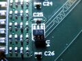
- N-MOSFET: 2x 2N7002 type MOSFET (marking: "72Y7"). Connected as "low-side" switch/LED driver and inverter.
Pinouts and connections:
JTAG header (FPGA):
The J3 pin header is a JTAG connector wired to the FPGA. The pins are (from left to right, the right-most pin, pin number 1, is square):
| 5 | 4 | 3 | 2 | 1 |
|---|---|---|---|---|
| GND | TMS | TCK | TDO | TDI |
Testpoints:
| T1 | T2 | T3 |
|---|---|---|
| 1.2V | 3.3V | GND (FX2) |
Cypress FX2:
| (FPGA 15, IO_L05P_3) PD5 | 1- | O | -56 | PD4 (FPGA 12, IO_L04P_3) |
| (FPGA 13, IO_L04N_3) PD6 | 2- | -55 | PD3 (FPGA 44, IO_L09N_2) | |
| (FPGA 10, IO_L03N_3) PD7 | 3- | -54 | PD2 (FPGA 5, IO_L02P_3) | |
| GND | 4- | -53 | PD1 (FPGA 4, IO_L01N_3) | |
| (FPGA 90, IO_0) CLKOUT | 5- | -52 | PD0 (FPGA 6, IO_L02N_3) | |
| VCC | 6- | -51 | *WAKEUP (3.3V) | |
| GND | 7- | -50 | VCC | |
| (FPGA 3, IO_L01P_3) RDY0/*SLRD | 8- | -49 | RESET# (3.3V via D2 (diode?)) | |
| (FPGA 16, IO_L05N_3) RDY1/*SLWR | 9- | -48 | GND | |
| AVCC | 10- | -47 | PA7 (FPGA 9, IO_L03P_3) | |
| (24MHz crystal) XTALOUT | 11- | -46 | PA6 (FPGA 30, IO_L04P_2) | |
| (24MHz crystal) XTALIN | 12- | -45 | PA5 (FPGA 85, IO_L03P_0) | |
| AGND | 13- | -44 | PA4 (FPGA 98, IO_L06P_0) | |
| AVCC | 14- | -43 | PA3 (FPGA 51, MISO) | |
| (USB D+) DPLUS | 15- | -42 | PA2 (FPGA 53, CCLK) | |
| (USB D-) DMINUS | 16- | -41 | PA1 (FPGA 48, INIT_B) | |
| AGND | 17- | -40 | PA0 (FPGA 54, DONE) | |
| VCC | 18- | -39 | VCC | |
| GND | 19- | -38 | CTL2 (FPGA 100, PROG_B) | |
| (FPGA 84, IO_L02N_0) *IFCLK | 20- | -37 | CTL1 (FPGA 97, IP_0) | |
| RESERVED | 21- | -36 | CTL0 (FPGA 94, IO_L05N_0) | |
| (EEPROM SCL) SCL | 22- | -35 | GND | |
| (EEPROM SDA) SDA | 23- | -34 | VCC | |
| VCC | 24- | -33 | GND | |
| (FPGA 40, IO_L08P_2) PB0 | 25- | -32 | PB7 (FPGA 93, IO_L05P_0) | |
| (FPGA 78, IO_L01N_0) PB1 | 26- | -31 | PB6 (FPGA 37, IO_L07N_2) | |
| (FPGA 77, IO_L01P_0) PB2 | 27- | -30 | PB5 (FPGA 41, IO_L08N_2) | |
| (FPGA 49, IO_L10N_2) PB3 | 28- | -29 | PB4 (FPGA 46, MOSI) |
Other FPGA connections:
| 28 | CH0 | 52 | CH8 |
|---|---|---|---|
| 29 | CH1 | 56 | CH9 |
| 32 | CH2 | 57 | CH10 |
| 33 | CH3 | 60 | CH11 |
| 34 | CH4 | 61 | CH12 |
| 36 | CH5 | 62 | CH13 |
| 43 | CH6 | 64 | CH14 |
| 50 | CH7 | 65 | CH15 |
| 73 | LED (active low) | ||
Photos
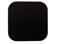
Device, front
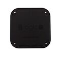
Device, bottom
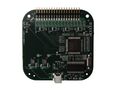
PCB, top
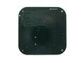
PCB, bottom
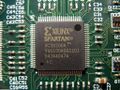
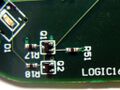
Xilinx XC3S200A
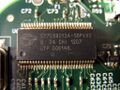
Cypress FX2LP
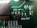
I2C EEPROM
ST DVIULC6-4SC6
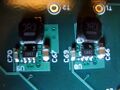
Voltage regulators
N-MOSFETs


Firmware
Firmware and FPGA bitstream usage
You can use the sigrok-fwextract-saleae-logic16 tool to extract (from the "Logic" Linux binary) the FX2 firmware and the FPGA bitstreams required for using the Saleae Logic16:
$ sigrok-fwextract-saleae-logic16 Logic
saved 5214 bytes to saleae-logic16-fx2.fw
saved 149516 bytes to saleae-logic16-fpga-18.bitstream
saved 149516 bytes to saleae-logic16-fpga-33.bitstream
Copy these files to the directory where your libsigrok installation expects them (usually /usr/local/share/sigrok-firmware) and they will be found and used automatically by the libsigrok saleae-logic16 driver.
Technical firmware details
The firmware for the FX2LP is embedded in the vendor application as a set of Intel HEX lines. Each line is uploaded individually with a separate control transfer. The firmware currently occupies the address range [0x0000-0x145d], but is uploaded out of order.
See Saleae Logic16/Firmware for more details on the vendor firmware.
Protocol
Sample format:
The samples (as received via USB) for the enabled probes (3, 6, 9, or 16) are organized as follows:
0xLL 0xLL 0xMM 0xMM 0xNN 0xNN 0xPP 0xPP 0xQQ 0xQQ 0xRR 0xRR ...
In the above example, 3 probes are enabled. For each probe there are 2 bytes / 16 bits (e.g. 0xLL 0xLL for probe 0), then the next probe's data is received (0xMM 0xMM for probe 1), then 0xNN 0xNN for probe 2. When 2 bytes have been received for all enabled probes, the process restarts with probe 0 again.
The 16 bits of data per probe seem to contain the pin state of the respective probe (1: high, 0: low) at 16 different sampling points/times (which ones depends on the samplerate).
Configuration:
Endpoint 1 is used for configuration of the analyzer. The transfers are "encrypted" using a simple series of additions and XORs. Two kinds of transfers are used; a 3 byte out transfer starting with 0x81 followed by a 1 byte in transfer, and a 4 byte out transfer starting with 0x80. It's quite plausible that these provide raw read/write access to memory locations.
| Channel number configuration | |
|---|---|
| 3 channels | 0x80 0x01 0x02 0x07 0x80 0x01 0x03 0x00 |
| 6 channels | 0x80 0x01 0x02 0x3f 0x80 0x01 0x03 0x00 |
| 9 channels | 0x80 0x01 0x02 0xff 0x80 0x01 0x03 0x01 |
| 16 channels | 0x80 0x01 0x02 0xff 0x80 0x01 0x03 0xff |
| Sampling frequency | |
|---|---|
| 500kHz | 0x80 0x01 0x0a 0x00 0x80 0x01 0x04 0xc7 |
| 1MHz | 0x80 0x01 0x0a 0x00 0x80 0x01 0x04 0x63 |
| 2MHz | 0x80 0x01 0x0a 0x00 0x80 0x01 0x04 0x31 |
| 4MHz | 0x80 0x01 0x0a 0x00 0x80 0x01 0x04 0x18 |
| 5MHz | 0x80 0x01 0x0a 0x00 0x80 0x01 0x04 0x13 |
| 8MHz | 0x80 0x01 0x0a 0x01 0x80 0x01 0x04 0x13 |
| 10MHz | 0x80 0x01 0x0a 0x00 0x80 0x01 0x04 0x09 |
| 12.5MHz | 0x80 0x01 0x0a 0x00 0x80 0x01 0x04 0x07 |
| 16MHz | 0x80 0x01 0x0a 0x01 0x80 0x01 0x04 0x09 |
| 25MHz | 0x80 0x01 0x0a 0x00 0x80 0x01 0x04 0x03 |
| 32MHz | 0x80 0x01 0x0a 0x01 0x80 0x01 0x04 0x04 |
| 40MHz | 0x80 0x01 0x0a 0x01 0x80 0x01 0x04 0x03 |
| 50MHz | 0x80 0x01 0x0a 0x00 0x80 0x01 0x04 0x01 |
| 80MHz | 0x80 0x01 0x0a 0x01 0x80 0x01 0x04 0x01 |
| 100MHz | 0x80 0x01 0x0a 0x00 0x80 0x01 0x04 0x00 |