Difference between revisions of "Pico Technology PicoScope 3206"
Uwe Hermann (talk | contribs) m |
(→Hardware: Information I gathered by looking at the PCB) |
||
| Line 11: | Line 11: | ||
* [http://www.xilinx.com/support/documentation/data_sheets/ds001.pdf Xilinx Spartan-II XC2S30] 30K gate FPGA | * [http://www.xilinx.com/support/documentation/data_sheets/ds001.pdf Xilinx Spartan-II XC2S30] 30K gate FPGA | ||
* Samsung K7N801845B-QC13 8MB SRAM | * Samsung K7N801845B-QC13 8MB SRAM | ||
* Cypress | * Cypress CY7C68013-56PVC (FX2) USB interface | ||
The brain of the device sits in the FX2. It does the USB communication, programs two DACs and the waveform generator, uploads the firmware into the FPGA, forwards some settings to the FPGA, and controls the seven relays, the input channel crossbar, and the power nets enable signals. The FPGA fetches samples from the ADCs, stores them in the SRAM and waits for the trigger signal. When done, it fetches the samples from the SRAM and gives them to the FX2. | |||
=== I2C === | |||
An ST24C02 EEPROM is directly connected to the FX2. It stores the USB ID and probably some calibration data. All other chips are behind an I2C gate (74VHC4052). The other I2C chips are | |||
* PCA9554A - 8 bit GPIO controller | |||
** IO0 and IO1 control the relays for channel B | |||
** IO2 and IO3 control the relays for channel A | |||
** IO4 drives the LED | |||
** IO5 decides which channel is routed to the AD8132+AD9215 behind the channel A connector | |||
** IO6 decides which channel is routed to the AD8132+AD9215 behind the channel B connector and the LT1715 for triggering | |||
** IO7 drives the relay to route the waveform generator to the EXT connector | |||
* MAX5822 - 2 channel DAC | |||
** Sets the trigger levels | |||
* AD5315 - 4 channel DAC | |||
** One output to each AD8132 | |||
** One output to the VREF pin of each AD9215 | |||
=== SPI === | |||
There is no SPI controller in the FX2. You have to do bit banging. | |||
* AD9833 - waveform generator | |||
** SDATA/SCLK/FSYNC is PD4/PD3/PD2 on the FX2 | |||
* XC2S30 - FPGA | |||
** DIN/CCLK/PROGRAM is PA1/PA7/PA0 on the FX2 | |||
=== Power Nets === | |||
* The voltage from the optional power supply is converted to 4.9V by an LM3578. This is combined with the nominal 5V from USB. This power rail sources the SP6650 for 3.3V and the secondary 5V power rail. | |||
* The 3.3V power rail is for the FX2, the EEPROM, the I2C gate, the MAX6424UK29, and the 555 timer. It also sources the secondary 3.3V power rail. It is always on. | |||
* The secondary 3.3V power rail is for the AD9833, the 25MHz oscillator, both AD9215s, and the LT1715. It is enabled while FX2 PD7 is low. | |||
* The secondary 5V power rail sources the LM2611 for -4.9V, the SP6650 for 2.5V, the MAX1896 for 6V, and both LP2981AIM5 for 4V. It is limited to about 7mA unless FX2 PD7 is low. | |||
* The 6V power rail is for the two SST5912s. It is enabled while FX2 PD5 is high. | |||
* The 2.5V power rail is for the FPGA and the SRAM. It is enabled while FX2 PD6 is high. | |||
* The -4.9V power rail is for the input channel and trigger signal conditioning, the waveform generator, and, what I call, the FPGA killer. It is enabled while FX2 PD5 is high. | |||
* One 4V power rail is for the input channel and trigger signal conditioning, the waveform generator. It is enabled while FX2 PD5 is high. | |||
* The other 4V power rail is for the AD5315, the MAX5822, the PCA9554, the LED and the relays. This one is always on. | |||
* FX2 PD5 also controls the I2C gate. | |||
* PD5/PD6/PD7 can be overridden by dip switches. | |||
=== FPGA === | |||
Thankfully this is only a two layer design without BGA components. On the top layer the 2.5V are distributed below the FPGA to all VCCINT and VCCO pins. Ground is fetched from the other side with vias. | |||
{| class="wikitable" | |||
|+FPGA IOs | |||
|- | |||
|Pin | |||
|Connected to | |||
|Pin | |||
|Connected to | |||
|Pin | |||
|Connected to | |||
|- | |||
| 3 | |||
| LT1715 out A (Trigger A or B) | |||
| 49 | |||
| SRAM /WE | |||
| 94 | |||
| SRAM D | |||
|- | |||
| 4 | |||
| LT1715 out B (Trigger EXT) | |||
| 50 | |||
| SRAM A19 | |||
| 95 | |||
| SRAM D | |||
|- | |||
| 6 | |||
| 25MHz oscillator | |||
| 51 | |||
| SRAM A | |||
| 96 | |||
| SRAM D | |||
|- | |||
| 7 | |||
| FX2 PD1 | |||
| 54 | |||
| SRAM A | |||
| 99 | |||
| SRAM D | |||
|- | |||
| 10 | |||
| FX2 PD0 | |||
| 56 | |||
| SRAM A | |||
| 100 | |||
| Test point | |||
|- | |||
| 11 | |||
| FX2 RDY1 | |||
| 57 | |||
| SRAM A | |||
| 102 | |||
| FPGA killer | |||
|- | |||
| 12 | |||
| FX2 WAKEUP | |||
| 58 | |||
| SRAM D | |||
| 103 | |||
| FPGA killer | |||
|- | |||
| 13 | |||
| FX2 PKTEND | |||
| 59 | |||
| SRAM D | |||
| 112 | |||
| AD9215-1 D9 | |||
|- | |||
| 18 | |||
| FX2 FLAGA | |||
| 60 | |||
| SRAM D | |||
| 113 | |||
| AD9215-1 D8 | |||
|- | |||
| 19 | |||
| FX2 FD4 | |||
| 62 | |||
| SRAM D | |||
| 114 | |||
| AD9215-1 D7 | |||
|- | |||
| 20 | |||
| FX2 FD5 | |||
| 63 | |||
| SRAM D | |||
| 115 | |||
| AD9215-1 D6 | |||
|- | |||
| 21 | |||
| FX2 FD6 | |||
| 65 | |||
| SRAM D | |||
| 117 | |||
| AD9215-1 D5 | |||
|- | |||
| 22 | |||
| FX2 FD7 | |||
| 66 | |||
| SRAM D | |||
| 118 | |||
| AD9215-1 D4 | |||
|- | |||
| 23 | |||
| FX2 FD0 | |||
| 67 | |||
| SRAM D | |||
| 120 | |||
| AD9215-1 D3 | |||
|- | |||
| 26 | |||
| FX2 FD1 | |||
| 68 | |||
| SRAM A | |||
| 121 | |||
| AD9215-1 D2 | |||
|- | |||
| 27 | |||
| FX2 FD2 | |||
| 69 | |||
| FX2 PA0 | |||
| 122 | |||
| AD9215-1 D1 | |||
|- | |||
| 28 | |||
| FX2 FD3 | |||
| 72 | |||
| Test point (DONE) | |||
| 123 | |||
| AD9215-1 D0 | |||
|- | |||
| 29 | |||
| FX2 IFCLK | |||
| 74 | |||
| SRAM A | |||
| 126 | |||
| AD9215-1 CLK | |||
|- | |||
| 31 | |||
| 555 out | |||
| 75 | |||
| SRAM A | |||
| 129 | |||
| AD9215-2 D9 | |||
|- | |||
| 37 | |||
| FX2 PA7 | |||
| 76 | |||
| SRAM A | |||
| 130 | |||
| AD9215-2 D8 | |||
|- | |||
| 38 | |||
| 10kOhm to CCLK? | |||
| 77 | |||
| SRAM A | |||
| 131 | |||
| AD9215-2 D7 | |||
|- | |||
| 39 | |||
| FX2 PA1 | |||
| 79 | |||
| SRAM A | |||
| 132 | |||
| AD9215-2 D6 | |||
|- | |||
| 40 | |||
| SRAM D | |||
| 80 | |||
| SRAM A | |||
| 133 | |||
| AD9215-2 D5 | |||
|- | |||
| 41 | |||
| SRAM D | |||
| 83 | |||
| SRAM A | |||
| 134 | |||
| AD9215-2 D4 | |||
|- | |||
| 43 | |||
| SRAM D | |||
| 84 | |||
| SRAM A | |||
| 136 | |||
| AD9215-2 D3 | |||
|- | |||
| 44 | |||
| SRAM D | |||
| 85 | |||
| SRAM A | |||
| 137 | |||
| AD9215-2 D2 | |||
|- | |||
| 46 | |||
| SRAM A | |||
| 86 | |||
| SRAM A | |||
| 139 | |||
| AD9215-2 D1 | |||
|- | |||
| 47 | |||
| SRAM A | |||
| 87 | |||
| SRAM A | |||
| 140 | |||
| AD9215-2 D0 | |||
|- | |||
| 48 | |||
| SRAM CLK | |||
| 93 | |||
| SRAM A | |||
| 141 | |||
| AD9215-2 CLK | |||
|} | |||
* As you can see only 16 data lines of the SRAM are connected. Two data pins are unused. This probably also means that the FPGA discards two of the data bits from the ADCs depending on the selected voltage range. | |||
* Pin 50 is an address pin only if the board is equipped with a bigger SRAM (K7N161831B). | |||
* I don't know what the 555 is used for. It looks like it in an astable configuration. | |||
* Have a good look at pin 102 and 103. They are connected to caps via 110 Ohm resistors. These caps are supplied by the -4.9V power rail via 100kOhm if both pins are inputs. '''This would probably kill part of the FPGA!''' So don't enable the -4.9V power rail until the FPGA has been loaded with a bitstream that drives these pins as output. Anyone knows if these pins serve any (other) purpose? Checking if -4.9V is enabled? | |||
== Photos == | == Photos == | ||
Revision as of 03:14, 19 February 2016

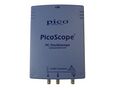
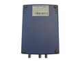
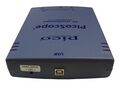
The Pico Technology PicoScope 3206 is a 200MHz analog bandwidth 200MS/s sampling USB oscilloscope.
See Pico Technology PicoScope 3206/Info for some more details (such as lsusb -v output) on the device.
See Pico Technology PicoScope 3000 series for information common to all devices in this series.
Hardware
- Xilinx Spartan-II XC2S30 30K gate FPGA
- Samsung K7N801845B-QC13 8MB SRAM
- Cypress CY7C68013-56PVC (FX2) USB interface
The brain of the device sits in the FX2. It does the USB communication, programs two DACs and the waveform generator, uploads the firmware into the FPGA, forwards some settings to the FPGA, and controls the seven relays, the input channel crossbar, and the power nets enable signals. The FPGA fetches samples from the ADCs, stores them in the SRAM and waits for the trigger signal. When done, it fetches the samples from the SRAM and gives them to the FX2.
I2C
An ST24C02 EEPROM is directly connected to the FX2. It stores the USB ID and probably some calibration data. All other chips are behind an I2C gate (74VHC4052). The other I2C chips are
- PCA9554A - 8 bit GPIO controller
- IO0 and IO1 control the relays for channel B
- IO2 and IO3 control the relays for channel A
- IO4 drives the LED
- IO5 decides which channel is routed to the AD8132+AD9215 behind the channel A connector
- IO6 decides which channel is routed to the AD8132+AD9215 behind the channel B connector and the LT1715 for triggering
- IO7 drives the relay to route the waveform generator to the EXT connector
- MAX5822 - 2 channel DAC
- Sets the trigger levels
- AD5315 - 4 channel DAC
- One output to each AD8132
- One output to the VREF pin of each AD9215
SPI
There is no SPI controller in the FX2. You have to do bit banging.
- AD9833 - waveform generator
- SDATA/SCLK/FSYNC is PD4/PD3/PD2 on the FX2
- XC2S30 - FPGA
- DIN/CCLK/PROGRAM is PA1/PA7/PA0 on the FX2
Power Nets
- The voltage from the optional power supply is converted to 4.9V by an LM3578. This is combined with the nominal 5V from USB. This power rail sources the SP6650 for 3.3V and the secondary 5V power rail.
- The 3.3V power rail is for the FX2, the EEPROM, the I2C gate, the MAX6424UK29, and the 555 timer. It also sources the secondary 3.3V power rail. It is always on.
- The secondary 3.3V power rail is for the AD9833, the 25MHz oscillator, both AD9215s, and the LT1715. It is enabled while FX2 PD7 is low.
- The secondary 5V power rail sources the LM2611 for -4.9V, the SP6650 for 2.5V, the MAX1896 for 6V, and both LP2981AIM5 for 4V. It is limited to about 7mA unless FX2 PD7 is low.
- The 6V power rail is for the two SST5912s. It is enabled while FX2 PD5 is high.
- The 2.5V power rail is for the FPGA and the SRAM. It is enabled while FX2 PD6 is high.
- The -4.9V power rail is for the input channel and trigger signal conditioning, the waveform generator, and, what I call, the FPGA killer. It is enabled while FX2 PD5 is high.
- One 4V power rail is for the input channel and trigger signal conditioning, the waveform generator. It is enabled while FX2 PD5 is high.
- The other 4V power rail is for the AD5315, the MAX5822, the PCA9554, the LED and the relays. This one is always on.
- FX2 PD5 also controls the I2C gate.
- PD5/PD6/PD7 can be overridden by dip switches.
FPGA
Thankfully this is only a two layer design without BGA components. On the top layer the 2.5V are distributed below the FPGA to all VCCINT and VCCO pins. Ground is fetched from the other side with vias.
| Pin | Connected to | Pin | Connected to | Pin | Connected to |
| 3 | LT1715 out A (Trigger A or B) | 49 | SRAM /WE | 94 | SRAM D |
| 4 | LT1715 out B (Trigger EXT) | 50 | SRAM A19 | 95 | SRAM D |
| 6 | 25MHz oscillator | 51 | SRAM A | 96 | SRAM D |
| 7 | FX2 PD1 | 54 | SRAM A | 99 | SRAM D |
| 10 | FX2 PD0 | 56 | SRAM A | 100 | Test point |
| 11 | FX2 RDY1 | 57 | SRAM A | 102 | FPGA killer |
| 12 | FX2 WAKEUP | 58 | SRAM D | 103 | FPGA killer |
| 13 | FX2 PKTEND | 59 | SRAM D | 112 | AD9215-1 D9 |
| 18 | FX2 FLAGA | 60 | SRAM D | 113 | AD9215-1 D8 |
| 19 | FX2 FD4 | 62 | SRAM D | 114 | AD9215-1 D7 |
| 20 | FX2 FD5 | 63 | SRAM D | 115 | AD9215-1 D6 |
| 21 | FX2 FD6 | 65 | SRAM D | 117 | AD9215-1 D5 |
| 22 | FX2 FD7 | 66 | SRAM D | 118 | AD9215-1 D4 |
| 23 | FX2 FD0 | 67 | SRAM D | 120 | AD9215-1 D3 |
| 26 | FX2 FD1 | 68 | SRAM A | 121 | AD9215-1 D2 |
| 27 | FX2 FD2 | 69 | FX2 PA0 | 122 | AD9215-1 D1 |
| 28 | FX2 FD3 | 72 | Test point (DONE) | 123 | AD9215-1 D0 |
| 29 | FX2 IFCLK | 74 | SRAM A | 126 | AD9215-1 CLK |
| 31 | 555 out | 75 | SRAM A | 129 | AD9215-2 D9 |
| 37 | FX2 PA7 | 76 | SRAM A | 130 | AD9215-2 D8 |
| 38 | 10kOhm to CCLK? | 77 | SRAM A | 131 | AD9215-2 D7 |
| 39 | FX2 PA1 | 79 | SRAM A | 132 | AD9215-2 D6 |
| 40 | SRAM D | 80 | SRAM A | 133 | AD9215-2 D5 |
| 41 | SRAM D | 83 | SRAM A | 134 | AD9215-2 D4 |
| 43 | SRAM D | 84 | SRAM A | 136 | AD9215-2 D3 |
| 44 | SRAM D | 85 | SRAM A | 137 | AD9215-2 D2 |
| 46 | SRAM A | 86 | SRAM A | 139 | AD9215-2 D1 |
| 47 | SRAM A | 87 | SRAM A | 140 | AD9215-2 D0 |
| 48 | SRAM CLK | 93 | SRAM A | 141 | AD9215-2 CLK |
- As you can see only 16 data lines of the SRAM are connected. Two data pins are unused. This probably also means that the FPGA discards two of the data bits from the ADCs depending on the selected voltage range.
- Pin 50 is an address pin only if the board is equipped with a bigger SRAM (K7N161831B).
- I don't know what the 555 is used for. It looks like it in an astable configuration.
- Have a good look at pin 102 and 103. They are connected to caps via 110 Ohm resistors. These caps are supplied by the -4.9V power rail via 100kOhm if both pins are inputs. This would probably kill part of the FPGA! So don't enable the -4.9V power rail until the FPGA has been loaded with a bitstream that drives these pins as output. Anyone knows if these pins serve any (other) purpose? Checking if -4.9V is enabled?
Photos
Device, top
Device, bottom

Device, front
Device, back
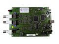
PCB, top
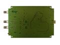
PCB, bottom


Protocol
See Pico_Technology_PicoScope_3000_series#Protocol.