Difference between revisions of "Kingst LA2016"
(link to protocol sub page for stuff that's too much for the device page) |
(more perceivable list of supported devices, stream mode is available and uncompressed) |
||
| Line 19: | Line 19: | ||
The current vendor is "Qingdao Kingst Electronics Co., Ltd." but older models are branded "Jiankun" rather than "Kingst". | The current vendor is "Qingdao Kingst Electronics Co., Ltd." but older models are branded "Jiankun" rather than "Kingst". | ||
Detailed specifications and the vendor software are available on the [http://www.qdkingst.com/en/products Kingst website]. | Detailed specifications and the vendor software are available on the [http://www.qdkingst.com/en/products Kingst website]. | ||
Despite its name (mostly for historic reasons) the '''kingst-la2016 driver supports other devices''' in the family, too: | |||
'''LA1010''' (untested), '''LA1016''' (lightly tested), '''LA2016''' (fully tested), '''LA5016''' (fully tested), and '''LA5032''' (untested). | |||
TODO Create a wiki page for the Kingst LA series, move common information there. Only keep device specific details and images in the LA2016 page. | |||
* '''Support Status:''' | * '''Support Status:''' | ||
** It is recommended to use recent software (at least mid November 2021, better February 2022), issues with LA2016 and LA1016 got addressed, and support for other devices has improved. | ** It is recommended to use recent software (at least mid November 2021, better February 2022), issues with LA2016 and LA1016 got addressed, and support for other devices has improved. | ||
** 2021-11-19 [https://github.com/sigrokproject/sigrok-firmware/pull/1 Open firmware] for the FX2 MCU is available for testing. FPGA bitstreams extraction from vendor software still is required. Behaviour of the vendor's and the open source MCU firmware shall be the same. | ** 2021-11-19 [https://github.com/sigrokproject/sigrok-firmware/pull/1 Open firmware] for the FX2 MCU is available for testing. FPGA bitstreams extraction from vendor software still is required. Behaviour of the vendor's and the open source MCU firmware shall be the same. | ||
* '''Known Issues:''' | * '''Known Issues:''' | ||
** PulseView allows the user to setup multiple edge triggers, but the analyser only supports one. Please only use one edge trigger to avoid undefined behaviour. Note the edge trigger can be combined with any number of level triggers. (gsi: Is this worth mentioning here? It's well understood that software use is contrained by hardware capabilities, all supported devices have constraints.) | ** PulseView allows the user to setup multiple edge triggers, but the analyser only supports one. Please only use one edge trigger to avoid undefined behaviour. Note the edge trigger can be combined with any number of level triggers. (gsi: Is this worth mentioning here? It's well understood that software use is contrained by hardware capabilities, all supported devices have constraints.) | ||
| Line 129: | Line 132: | ||
Acquisition is completely driven by the device's hardware. A configuration gets sent to the device, specifying enabled channels, samplerate, samples count, trigger parameters. The hardware acquires data from the logic probes and writes it to local RAM. After the acquisition has completed, the host can download the captured data. Hardware compression is transparent, some 50MSa are guaranteed (model dependent). Oversampling and slowly changing input data can result in the ability to squeeze a few GSa into RAM before the memory capacity is exhausted, this heavily depends on the input signal's pattern. | Acquisition is completely driven by the device's hardware. A configuration gets sent to the device, specifying enabled channels, samplerate, samples count, trigger parameters. The hardware acquires data from the logic probes and writes it to local RAM. After the acquisition has completed, the host can download the captured data. Hardware compression is transparent, some 50MSa are guaranteed (model dependent). Oversampling and slowly changing input data can result in the ability to squeeze a few GSa into RAM before the memory capacity is exhausted, this heavily depends on the input signal's pattern. | ||
All devices in the family support streaming mode. Most of them in addition to or as an alternative to local storage before download, the memory-less LA1010 as the only supported mode of operation. All of the preparation (device identification, firmware download, acquisition setup, sample data upload from USB endpoint 6) is identical to "normal mode" as the vendor calls it. But sample data upload immediately starts when the acquisition gets initiated. The device will neither use local memory for buffering, to compensate for bursts in the input data and slow USB communication to the PC. Nor will the device apply RLE compression on the sample data, bits only get shifted in ways similar to Saleae-Logic16 to reduce the amount of USB traffic while uncompressed data gets communicated. Successful reception of sample data in streaming mode heavily depends on the whole chain from the device to the host application and its capability to process the steady USB communication at high Mbps rates. The vendor software assumes a limit of some 300Mbps (sample rate multiplied by the number of enabled channels). | |||
Many of the FPGA registers are read-only or write only, which prevents reading back a configuration that previously was written to the device. When registers support read and write, their meaning differs depending on the direction of data exchange. | Many of the FPGA registers are read-only or write only, which prevents reading back a configuration that previously was written to the device. When registers support read and write, their meaning differs depending on the direction of data exchange. | ||
Revision as of 01:26, 23 February 2022
 | |
| Status | supported |
|---|---|
| Source code | kingst-la2016 |
| Channels | 16 |
| Samplerate | 200MHz max. |
| Samplerate (state) | State analysis not supported |
| Triggers |
Level (multiple channels) Edge (one channel) |
| Min/max voltage | -50V — 50V |
| Threshold voltage |
Configurable: -4V—4V, min step 0.01V |
| Memory |
128MByte DDR2 SDRAM 40M—10G samples |
| Compression | Yes |
| Website | qdkingst.com |
The Kingst LA2016 is a USB-based, 16-channel logic analyser with 200MHz maximum sampling rate and 128MB sample memory. Other devices in the series support differing samplerates (100/200/500MHz), channel counts (16 or 32), and memory sizes (1/2/4Gib). The current vendor is "Qingdao Kingst Electronics Co., Ltd." but older models are branded "Jiankun" rather than "Kingst". Detailed specifications and the vendor software are available on the Kingst website.
Despite its name (mostly for historic reasons) the kingst-la2016 driver supports other devices in the family, too: LA1010 (untested), LA1016 (lightly tested), LA2016 (fully tested), LA5016 (fully tested), and LA5032 (untested). TODO Create a wiki page for the Kingst LA series, move common information there. Only keep device specific details and images in the LA2016 page.
- Support Status:
- It is recommended to use recent software (at least mid November 2021, better February 2022), issues with LA2016 and LA1016 got addressed, and support for other devices has improved.
- 2021-11-19 Open firmware for the FX2 MCU is available for testing. FPGA bitstreams extraction from vendor software still is required. Behaviour of the vendor's and the open source MCU firmware shall be the same.
- Known Issues:
- PulseView allows the user to setup multiple edge triggers, but the analyser only supports one. Please only use one edge trigger to avoid undefined behaviour. Note the edge trigger can be combined with any number of level triggers. (gsi: Is this worth mentioning here? It's well understood that software use is contrained by hardware capabilities, all supported devices have constraints.)
- The device supports an input threshold range of -4.0V to +4.0V, but the sigrok driver currently implements a limited set of discrete values. Which covers all popular logic families (0.8V to 5.0V), but omits zero crossing as well as negative values. Which should not be too limiting a constraint.
- The vendor's hardware design does not allow to read back previously written configurations. The software always needs to assign a set of default values upon startup, and cannot continue using a previously applied configuration.
- Unplugging the analyser and then attempting to start a capture causes PulseView to crash.
See Kingst LA2016/Info for more details (USB identification).
Hardware
This logic analyser has been on the market since around 2012 and there are a few different revisions of it. The schematic has been reverse engineered from a unit purchased in 2020 containing a PCB marked as v1.3.0. The circuitry of older PCBs is similar but may have different voltage regulators, different input channel routing to the FPGA, and lack the input threshold adjustment.
The LA1016 uses identical hardware with a different FPGA bitstream which limits the sample rate to 100MHz maximum.
All of these devices use the same firmware for the FX2LP MCU but there are four different FPGA bitstreams; i.e. LA1016 & LA2016 bitstreams and the older versions of these (to swap some of the input channels as required by PCB routing changes). Once the FX2LP firmware has been loaded, a 'magic number' is read from EEPROM which identifies the device and thus allows the correct FPGA bitstream to be loaded.
Note that the LA1016 cannot be boosted to 200MHz by changing the 'magic number' or the FPGA bitstream. When the FPGA initialises, its reads 16 bytes from U10 which are used to authenticate the bitstream; these bytes are different for 100 and 200MHz devices. Furthermore, the OEM software performs a challenge-response with U10 to authenticate the logic analyser as genuine 'Kingst'. The good news is that U10 does not impact sigrok support in any way and we don't need to communicate with it.
Main components and their function:
- MCU Cypress FX2LP
- This MCU only has volatile memory and in this implementation it's firmware is loaded from the host by the application software.
- Either the OEM firmware or open source firmware can be used.
- In essence, it just performs data moving operations:
- Endpoint 0 to EEPROM read/write
- Endpoint 0 to SPI read/write for FPGA control registers
- Endpoint 2 bulk out to SPI for loading FPGA bitstream
- Endpoint 6 bulk in to read capture data from FPGA/SDRAM
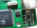
- EEPROM Atmel AT24C02 2Kbit
- This non-volatile memory stores:
- VID:PID which is 77a1:01a2 for LA1016 and LA2016 devices
- 'magic number' to identify model and revision
- purchase date (presumably for warranty claims)
- other information related to U10 but not of interest to sigrok
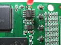
- FPGA Altera EP4CE6
- Currently requires the OEM bitstream.
- Has a bank of approximately 60 byte-wide registers accessed via SPI which are used to contol FPGA functions.
- Captures 16 input channels, performs compression (run length encoding, 16bit sample plus 8 bit repetition count).
- Stores samples to SDRAM (or streams direct to USB but we don't implement that method).
- Interestingly, this device (6K LE) shares the same die as the next up device EP4CE10 (10K LE) and can be programmed as such. However, functionality would not be guaranteed as CE6 devices may be CE10 rejects.
- If open source FPGA code were to become available there would be capacity to experiment with more advanced triggers, such as pattern trigger for SPI or I2C.
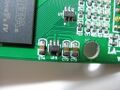
- SDRAM Samsung DDR2
- Samples are stored as 3 bytes (16bit sample plus 8 bit repetition count).
- A 'transfer packet' for upload is 16 bytes = 5 compressed samples plus a sequence number byte.
- Burst read/write for this SDRAM is up to 16 bytes, which matches the transfer packet size and is likely used for all SDRAM read/writes.
- U10 Kingst Authentication Device
- Not used by sigrok.
- Provides fixed bytes identifier to FPGA for bitstream validation (either LA1016 100MHz or LA2016 200MHz bitstream)
- Provides challenge-response rolling-code for OEM software to authenticate the device as genuine 'Kingst'
Datasheets:
- U1 EP4CE6F17C8N Cyclone IV E FPGA
- U2,4,5,7 PDWL050019 TVS Diode Array
- U3 CY7C68013A-100AXC EZUSB MCU
- U6,U8 SGM2019 Linear Regulator
- U9 AT24C02 EEPROM 2kbit
- U10 (device not identified, small MCU of some type)
- U11 K4T1G164QG-BCF8, DDR2 SDRAM, obsolete
- U12,U13 SGM6013 Switch-mode Regulator
- U14 SGM8272 Dual Op-amp
- U15 TPS60403 Charge Pump Voltage Inverter
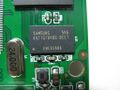
Photos
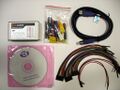
Package contents
Paper
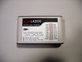
Device, top
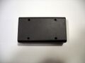
Device, bottom
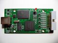
PCB, top
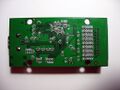
PCB, bottom
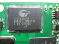
Cypress FX2
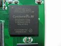
Altera Cyclone IV
Samsung K4T1G164QG
Atmel 24C02N
Unmarked IC
PFNI


Protocol
Several devices share the same USB identification (VID and PID). The PID determines which FX2 MCU firmware to upload to the device. Once the MCU firmware is in place (which involves USB renumeration), USB communication can access EEPROM content, which allows to identify the device type. Which determines the device's capabilities (maximum samplerate, channel count, memory depth), and the FPGA bitstream to upload to the device. The FPGA logic will automatically verify its matching the device hardware by communicating to IC U10, loading non-matching bitstreams will not enable features which the device does not provide in its proper configuration.
The device's firmware provides two (three) USB endpoints. EP2 is write only and is used to upload FPGA bitstreams. EP6 is read only and downloads captured sample data by means of USB bulk transfers. EP0 supports USB control transfers to configure the device and supervise its operation.
Acquisition is completely driven by the device's hardware. A configuration gets sent to the device, specifying enabled channels, samplerate, samples count, trigger parameters. The hardware acquires data from the logic probes and writes it to local RAM. After the acquisition has completed, the host can download the captured data. Hardware compression is transparent, some 50MSa are guaranteed (model dependent). Oversampling and slowly changing input data can result in the ability to squeeze a few GSa into RAM before the memory capacity is exhausted, this heavily depends on the input signal's pattern.
All devices in the family support streaming mode. Most of them in addition to or as an alternative to local storage before download, the memory-less LA1010 as the only supported mode of operation. All of the preparation (device identification, firmware download, acquisition setup, sample data upload from USB endpoint 6) is identical to "normal mode" as the vendor calls it. But sample data upload immediately starts when the acquisition gets initiated. The device will neither use local memory for buffering, to compensate for bursts in the input data and slow USB communication to the PC. Nor will the device apply RLE compression on the sample data, bits only get shifted in ways similar to Saleae-Logic16 to reduce the amount of USB traffic while uncompressed data gets communicated. Successful reception of sample data in streaming mode heavily depends on the whole chain from the device to the host application and its capability to process the steady USB communication at high Mbps rates. The vendor software assumes a limit of some 300Mbps (sample rate multiplied by the number of enabled channels).
Many of the FPGA registers are read-only or write only, which prevents reading back a configuration that previously was written to the device. When registers support read and write, their meaning differs depending on the direction of data exchange.
See Kingst LA2016/Protocol for more developer notes and captures that were taken during protocol research.
Firmware
In order to use this device you need to extract the firmware/FPGA files from the vendor software (Linux download) using the sigrok-fwextract-kingst-la2016 script from the sigrok-util repo and place them in one of the usual places where libsigrok expects firmware files:
$ ./sigrok-fwextract-kingst-la2016 KingstVIS/KingstVIS
saved 5430 bytes to kingst-la-01a2.fw (crc32=720551a9)
saved 178362 bytes to kingst-la2016a1-fpga.bitstream (crc32=7cc894fa)
saved 178542 bytes to kingst-la2016-fpga.bitstream (crc32=20694ff1)
saved 178379 bytes to kingst-la1016a1-fpga.bitstream (crc32=166866be)
saved 178151 bytes to kingst-la1016-fpga.bitstream (crc32=7db70001)