Difference between revisions of "Hantek 1008C"
Martinloren (talk | contribs) m |
m (typo) |
||
| (12 intermediate revisions by 2 users not shown) | |||
| Line 7: | Line 7: | ||
| samplerate = 2.4MS/s (see notes) | | samplerate = 2.4MS/s (see notes) | ||
| samplerate_state = ? | | samplerate_state = ? | ||
| triggers = | | triggers = edge on either channel | ||
| voltages = | | voltages = ±500mV / ±20V | ||
| memory = | | memory = 4K samples, 12bits each | ||
| compression = ? | | compression = ? | ||
| website = [http://www.hantek.com/ | | website = [http://www.hantek.com.cn/en/ProductDetail_13_13170.html hantek.com] | ||
}} | }} | ||
| Line 26: | Line 26: | ||
* '''8-bit shift register with 3-state output:''' 74HC595 (3 total) | * '''8-bit shift register with 3-state output:''' 74HC595 (3 total) | ||
* '''Dual opamp:''' in MSOP-8 package, Texas Instruments unknown model (chip markings "TI 25 AVG") (1 per analog channel) | * '''Dual opamp:''' in MSOP-8 package, Texas Instruments unknown model (chip markings "TI 25 AVG") (1 per analog channel) | ||
1M impedance, DC coupling | |||
ships with one high pressure ignition probe (inductive) | |||
more recent board revision ("Mini DSO V1.00.14 // 2018-11") | |||
* STM32F103C8T6 | |||
* AMS1117-3.3 LDO plus (not identified) SMPS U427, no barrel jack, only USB-B | |||
* 8x NXP 74HC4051D, 8x TI 86 AVG (per analog channel) | |||
* 1x TI HC244 (for digital outputs) | |||
* 1x TI 86 AVG (near IDC pin header, A0/A1 signals) | |||
* 3x HC595 | |||
== Photos == | == Photos == | ||
=== V1.00.4 2012-03 === | |||
<gallery> | <gallery> | ||
| Line 49: | Line 63: | ||
File:Hantek_1008C_IC_ti25avg.jpg|<small>TI25AVG</small> | File:Hantek_1008C_IC_ti25avg.jpg|<small>TI25AVG</small> | ||
File:Hantek_1008C_input_frontend.jpg|<small>Analog input circuit</small> | File:Hantek_1008C_input_frontend.jpg|<small>Analog input circuit</small> | ||
</gallery> | |||
=== V1.00.12 2018-11 === | |||
There is another version ("Mini DSO V1.00.12 // 2018-11") which differs from the images above: Comes in a pouch, ships with eight BNC to alligator cables, lacks a barrel jack, LED position has moved, rubber bumpers around case edges, no silkscreen labels on the case, signal names "engraved", teardown yet to be done. See the (updated) vendor's product page to get an idea. | |||
<gallery> | |||
File:Hantek-1008c-pcb-top.png|<small>PCB top</small> | |||
File:Hantek-1008c-pcb-ch123.png|<small>PCB top, channels 1-3</small> | |||
File:Hantek-1008c-pcb-ch3456.png|<small>PCB top, channels 3-6</small> | |||
File:Hantek-1008c-pcb-ch78.png|<small>PCB top, channels 7-8</small> | |||
File:Hantek-1008c-pcb-reg-mcu-gen.png|<small>PCB top, regulation, MCU, generator, pin expander</small> | |||
File:Hantek-1008c-pcb-bottom.png|<small>PCB bottom</small> | |||
File:Hantek-1008c-case-blinds-1.png|<small>case walls, connector labels</small> | |||
File:Hantek-1008c-case-blinds-2.png|<small>case walls, generator pinout</small> | |||
</gallery> | </gallery> | ||
| Line 57: | Line 86: | ||
=== List of commands (incomplete) === | === List of commands (incomplete) === | ||
* A0 -> set number of channel enabled (ie. A0 02: 2 channels are enabled) | |||
* AA -> set which channel to enable (ie. AA 01 01 00 00 00 00 00 00 enable channel 1 and 2) | * AA -> set which channel to enable (ie. AA 01 01 00 00 00 00 00 00 enable channel 1 and 2) | ||
* A2 -> set voltage level for each channel (ie. A2 03 03 03 03 03 03 03 03 apply +- | * A2 -> set voltage level for each channel (ie. A2 03 03 03 03 03 03 03 03 apply +-20V range on each channel) | ||
* A3 -> set sampling rate (ie. A3 | * A3 -> set sampling rate (ie. A3 00 set highest sampling rate) | ||
* AC -> set sampling rate (ie. AC 07 D0 00 03 42 00 03 42 set highest sampling rate for 2 channels enabled = 1.2MS/s) | |||
* AB -> set trigger level (ie. AB 08 00) | |||
* C1 -> set trigger source and slope (ie. C1 00 00 for Channel 1, rising slope, C1 01 01 for Channel 2, falling slope) | |||
* F3 -> hardware ping (required to send regularly also when acquisition is stoped, otherwise the hardware disconnect) | |||
=== Sample of initialization cycle === | === Sample of initialization cycle === | ||
| Line 99: | Line 133: | ||
* Sample rate: maximum measured 2.4MS/s if just 1 channel is enabled. Drop down to 1.2MS/s if enable 2 channels. | * Sample rate: maximum measured 2.4MS/s if just 1 channel is enabled. Drop down to 1.2MS/s if enable 2 channels. | ||
* Acquisition: on each scan acquire 4000 samples from 2 buffers (2000 samples each buffer) | * Acquisition: on each scan acquire 4000 bytes (2000 samples) from 2 buffers (2000 samples each buffer) | ||
* Voltage Selector: the most reliable voltage selection is +/-20V, lower hardware voltages present strong non-linearity which make useless the full ADC range of the device (for example +/-500mV range is linear just in the range +500mV -> -80mV. | |||
* Zero offset on ADC is strongly temperature dependent. It drops fast after the device is turned on (even around 50mV on a scale of +-20V). It is suggested to perform the Zero offset calibration and to use this instrument after few minutes that is on, when the temperature stabilize. | |||
== Resources == | == Resources == | ||
* [http://www.hantek.com.cn/en/ProductDetail_13_13170.html vendor's product page] | |||
* [http://www.hantek.com/Product/Hantek1008/Hantek1008_Manual.pdf Manual] | * [http://www.hantek.com/Product/Hantek1008/Hantek1008_Manual.pdf Manual] | ||
* [http://www.hantek.com.cn/Product/Hantek1008/Hantek1008_V1.0.8.zip Vendor software] | * [http://www.hantek.com.cn/Product/Hantek1008/Hantek1008_V1.0.8.zip Vendor software] | ||
* [https://forums.ni.com/t5/LabVIEW/Hantek-1008C-data-type/td-p/3240415 Decode .DRC data format] | * [https://forums.ni.com/t5/LabVIEW/Hantek-1008C-data-type/td-p/3240415 Decode .DRC data format] | ||
* [https://github.com/giwig/hantek1008C giwig hantek1008C] and [https://github.com/mfg92/hantek1008py mfg hantek1008py] github repositories, Apache licensed Python code (somehow related to or derived from each other?) | |||
* [https://www.youtube.com/watch?v=OaPVTmd5ins A DIY solution to providing hardware based AC COUPLING to HANTEK 1008] | |||
* [https://www.youtube.com/watch?v=BjPUbO-U-VA Make a DIY AC Coupling Adapter for Hantek 1008C] | |||
* [https://www.youtube.com/watch?v=gCd4bbuFPNA&t=79s Make an external DIY AC Coupler] | |||
[[Category:Device]] | [[Category:Device]] | ||
[[Category:Oscilloscope]] | [[Category:Oscilloscope]] | ||
[[Category:Planned]] | [[Category:Planned]] | ||
Latest revision as of 19:56, 12 June 2020
 | |
| Status | planned |
|---|---|
| Channels | 8 |
| Samplerate | 2.4MS/s (see notes) |
| Samplerate (state) | ? |
| Triggers | edge on either channel |
| Min/max voltage | ±500mV / ±20V |
| Memory | 4K samples, 12bits each |
| Compression | ? |
| Website | hantek.com |
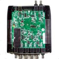
The Hantek 1008C is a USB-based 8-channel oscilloscope (sampling resolution: 12bits on each channel), with 8 channel digital pattern generator.
See Hantek 1008C/Info for some more details (such as lsusb -vvv output) on the device.
Hardware
- CPU: ST Microelectronics STM32F103C6T6A
- Low-dropout voltage regulator: Advanced Monolithic Systems AMS1117-3.3
- 8-channel analog multiplexer/demultiplexer: NXP Semiconductor 74HCT4051D (1 per analog channel)
- Octal 3-state buffer: Fairchild Semiconductor MM74HC244SJ (in the path of digital outputs)
- 8-bit shift register with 3-state output: 74HC595 (3 total)
- Dual opamp: in MSOP-8 package, Texas Instruments unknown model (chip markings "TI 25 AVG") (1 per analog channel)
1M impedance, DC coupling
ships with one high pressure ignition probe (inductive)
more recent board revision ("Mini DSO V1.00.14 // 2018-11")
- STM32F103C8T6
- AMS1117-3.3 LDO plus (not identified) SMPS U427, no barrel jack, only USB-B
- 8x NXP 74HC4051D, 8x TI 86 AVG (per analog channel)
- 1x TI HC244 (for digital outputs)
- 1x TI 86 AVG (near IDC pin header, A0/A1 signals)
- 3x HC595
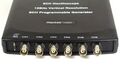
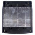
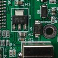
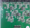
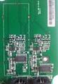
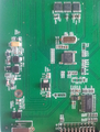
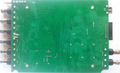
Photos
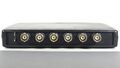
V1.00.4 2012-03
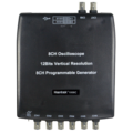
Device, top
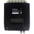
Device, bottom
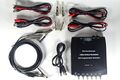
Package contents
Device, front
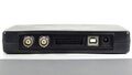
Device, back
Front inputs

Void if removed sticker
Top cover
Top cover removed
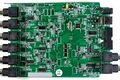
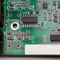
PCB, top
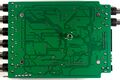
PCB, bottom
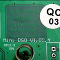
PCB revision, v1.00.4
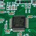
Main CPU, STM32F1
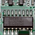
74HC4051D
AMS1117 3.3V LDO
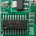
HC224SJ
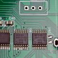
HC595
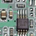
TI25AVG
Analog input circuit


V1.00.12 2018-11
There is another version ("Mini DSO V1.00.12 // 2018-11") which differs from the images above: Comes in a pouch, ships with eight BNC to alligator cables, lacks a barrel jack, LED position has moved, rubber bumpers around case edges, no silkscreen labels on the case, signal names "engraved", teardown yet to be done. See the (updated) vendor's product page to get an idea.
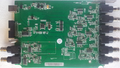
PCB top
PCB top, channels 1-3
PCB top, channels 3-6
PCB top, channels 7-8
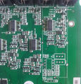
PCB top, regulation, MCU, generator, pin expander
PCB bottom
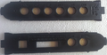
case walls, connector labels
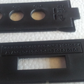
case walls, generator pinout


Protocol
Need to continuously send commands to the OUT Endpoint, and for each command receive the result from the IN Endpoint (both Endpoints can transfer max 64 bytes). The device got logically disconnected automatically if not receive any command after 7 seconds.
List of commands (incomplete)
- A0 -> set number of channel enabled (ie. A0 02: 2 channels are enabled)
- AA -> set which channel to enable (ie. AA 01 01 00 00 00 00 00 00 enable channel 1 and 2)
- A2 -> set voltage level for each channel (ie. A2 03 03 03 03 03 03 03 03 apply +-20V range on each channel)
- A3 -> set sampling rate (ie. A3 00 set highest sampling rate)
- AC -> set sampling rate (ie. AC 07 D0 00 03 42 00 03 42 set highest sampling rate for 2 channels enabled = 1.2MS/s)
- AB -> set trigger level (ie. AB 08 00)
- C1 -> set trigger source and slope (ie. C1 00 00 for Channel 1, rising slope, C1 01 01 for Channel 2, falling slope)
- F3 -> hardware ping (required to send regularly also when acquisition is stoped, otherwise the hardware disconnect)
Sample of initialization cycle
- B0
- F3
- B901BF040000
- B700
- BB0800
- B5
- B6
- E5
- F7
- F8
- FA
- F5
- A008
- AA0101010101010101
- A311
- C10000
- A70000
- AC01F40009C50009C5
Start of waiting cycle for data to be ready into the buffers
- F3
- A2 01 01 01 01 01 01 01 01
- A4 01
- C0
- C2
- A5 5A
- A5 5A
Buffers Reading Cycle
- C6 02 (return Buffer 1 size)
- A6 02 (acquire 64 bytes, 32 samples of 12 bits each, repeated 60 times get 2000 samples)
- C6 03 (return Buffer 2 size)
- A6 03 (acquire 64 bytes, 32 samples of 12 bits each, repeated 60 times get 2000 samples)
Notes
- Sample rate: maximum measured 2.4MS/s if just 1 channel is enabled. Drop down to 1.2MS/s if enable 2 channels.
- Acquisition: on each scan acquire 4000 bytes (2000 samples) from 2 buffers (2000 samples each buffer)
- Voltage Selector: the most reliable voltage selection is +/-20V, lower hardware voltages present strong non-linearity which make useless the full ADC range of the device (for example +/-500mV range is linear just in the range +500mV -> -80mV.
- Zero offset on ADC is strongly temperature dependent. It drops fast after the device is turned on (even around 50mV on a scale of +-20V). It is suggested to perform the Zero offset calibration and to use this instrument after few minutes that is on, when the temperature stabilize.
Resources
- Decode .DRC data format
- giwig hantek1008C and mfg hantek1008py github repositories, Apache licensed Python code (somehow related to or derived from each other?)