Difference between revisions of "HT USBee-AxPro"
Uwe Hermann (talk | contribs) |
PaulFertser (talk | contribs) (→Hardware: information regarding analog input) |
||
| Line 50: | Line 50: | ||
|} | |} | ||
=== Analog frontend === | |||
[http://sigrok.org/wiki/File:Ht-usbee-axpro_analog_schematics.svg Schematics] | |||
Notes: | |||
* Some devices have R2 = 66.5 Ohms instead of kiloohms, this basically limits the range to -3.3V — +3.3V | |||
* TLC5510 is used with ~3.3V "reference" from LDO output which is both out of the allowed range and is a major source of inaccuracy | |||
* Some devices (probably those that do not have U5 populated) produce bogus min and max spikes when measuring certain voltages, this can probably be remedied by adding small (on the order of 10s pF) capacitance to U5 Vcc and GND pins or to the ADC CLK line | |||
* This board was apparently designed by people lacking EE knowledge, do not expect much from it | |||
'''HT_V6.0''': | '''HT_V6.0''': | ||
Revision as of 23:41, 16 July 2016
 | |
| Status | supported |
|---|---|
| Source code | fx2lafw |
| Channels | 8 + 1 |
| Samplerate | 24MHz |
| Samplerate (state) | — |
| Triggers | none (SW-only) |
| Min/max voltage |
Digital: -1V — +6V Analog: ±10V (±20V max) |
| Threshold voltage | Fixed: VIH=1.6V, VIL=1.4V |
| Memory | none |
| Compression | none |
| Website | aliexpress.com |
The HT USBee-AxPro is a USB-based, 8-channel logic analyzer with up to 24MHz sampling rate, with 1 additional analog channel.
It is able to switch between USBee AX-Pro, Salea Logic and Altera USB blaster mode via a button. When pressing the button the USB VID/PID changes.
It is a clone of the CWAV USBee AX-Pro.
In sigrok, we use the open-source fx2lafw firmware for this logic analyzer.
See HT USBee-AxPro/Info for some more details (such as lsusb -v output) on the device.
Hardware
HT2013 V5.00:
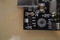
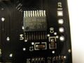
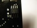
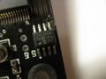
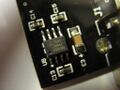
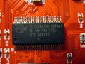
- Main chip: Cypress CY7C68013A-56SSOP (FX2LP)
- 64Kbit I²C EEPROM: Microchip 24LC641
- 2Kbit I²C EEPROM: Microchip 24LC02B
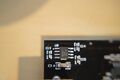
- Auxiliary 8051 chip: ST STM8S003F3 (used for handling the button)
- Supply voltage regulator: Advanced Monolithic Systems AMS1117-3.3
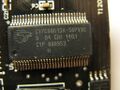
- Analog-to-digital converter: Texas Instruments TLC5510I
- Analog input amplifiers: Analog Devices AD8065 (SMD marking "HRA")
- Analog amplifiers negative supply: Intersil ICL7660 (7660 AIBAZ V120428A)
- Crystal: 24MHz
FX2LP pin mappings
| # | Pin | Destination | Remark |
|---|---|---|---|
| CTL2 | ADC_CLK | ADC clock | |
| PD0..7 | ADC_D1..8 | ADC data output |
Analog frontend
Notes:
- Some devices have R2 = 66.5 Ohms instead of kiloohms, this basically limits the range to -3.3V — +3.3V
- TLC5510 is used with ~3.3V "reference" from LDO output which is both out of the allowed range and is a major source of inaccuracy
- Some devices (probably those that do not have U5 populated) produce bogus min and max spikes when measuring certain voltages, this can probably be remedied by adding small (on the order of 10s pF) capacitance to U5 Vcc and GND pins or to the ADC CLK line
- This board was apparently designed by people lacking EE knowledge, do not expect much from it
HT_V6.0:
- ...
Pin mappings
The FX2 CTL2 and PD0..7 pins are mapped exactly like the HT2013 V5.00 version. The TLC5510I OE# pin is tied to GND.
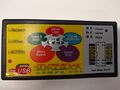
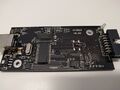
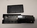
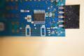
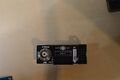
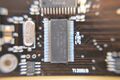
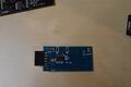
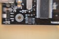
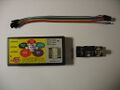
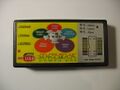
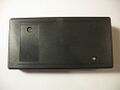
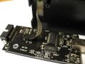
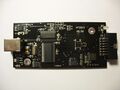
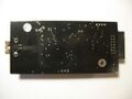
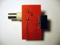
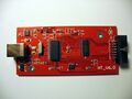
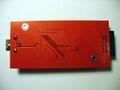
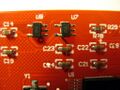
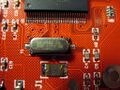
Photos
HT2013 V5.00:
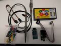
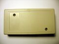
Device package
Case, front
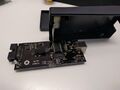
Device
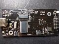
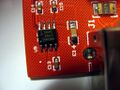
PCB, front
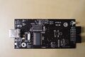
PCB, front
PCB, front
PCB, back
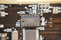
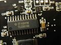
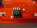
TLC5510I
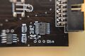
STM8 1
STM8 2
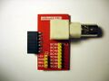
Probe adaptor
FX2
Expansion board
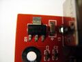
AMS1117
7660
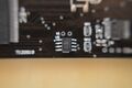
24LC64
24LC02B


HT2013 V5.00 (no blue button PCB):
Package contents
Device, top
Device, bottom
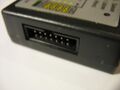
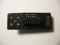
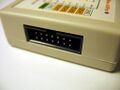
Connector
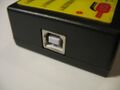
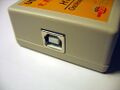
USB
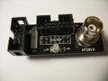
Analog connector, top
Analog connector, bottom
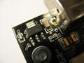
Button connector
PCB, top
PCB, bottom
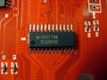
Cypress FX2
ST STM8S003F3
Microchip 24LC64I
Microchip 24LC02BI
Intersil ICL7660
TI TLC5510I
AMS1117-3.3


HT_V6.0:
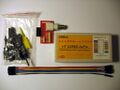
Package contents
Device, top
Device, bottom
Connector
USB
Analog adapter, top
Analog adapter, bottom
PCB, top
PCB, bottom
Cypress FX2
Microchip 24LC02B
TI TLC5510I
Intersil ICL7660S
AMS1117-3.3
HRA
24MHz crystal


Protocol
Since we use the open-source fx2lafw firmware for this device, we don't need to know the protocol.