KingST KQS3506-LA16100
 | |
| Status | supported |
|---|---|
| Source code | saleae-logic16 |
| Channels | 3/6/9/16 |
| Samplerate | 100/50/32/16MHz |
| Samplerate (state) | — |
| Triggers | none (SW-only) |
| Min/max voltage | -0.9V — 6V |
| Threshold voltage |
configurable: for 1.8V to 3.6V systems: VIH=1.4V, VIL=0.7V for 5V systems: VIH=3.6V, VIL=1.4V |
| Memory | none |
| Compression | yes |
| Website | taobao.com |
The KingST KQS3506-LA16100 is a USB-based, 16-channel logic analyzer with 100/50/32/16MHz sampling rate (at 3/6/9/16 enabled channels).
This is a clone of the Saleae Logic16.
See KingST KQS3506-LA16100/Info for more details (such as lsusb -v output) about the device.
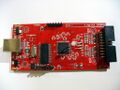
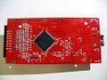
Hardware
- FPGA: Xilinx Spartan-3A XC3S200A, 200K gates (datasheet)
- CPLD: Altera EPM3032A, 600 gates, 32 macrocells (datasheet, pinout).
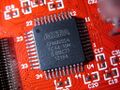
- USB interface chip: Cypress CY7C68013A-56PVXC (FX2LP) (datasheet)
- I2C EEPROM: Microchip 24LC02B (datasheet)
- 3.3V voltage regulator: Advanced Monolithic Systems AMS1117-3.3 (datasheet, older datasheet)
- 1.2V voltage regulator: Advanced Monolithic Systems AMS1117-1.2 (datasheet, older datasheet)
- Crystal: 24.000
Pinouts and connections:
I2C EEPROM:
The Microchip 24LC02B is connected to the Cypress FX2. The WP pin of the EEPROM can be jumpered to low or high, in order to write-protect it (or not). The address pins (A0-A2) are all connected to GND, which makes the I2C slave address of the EEPROM 0x50.
| (GND) A0 | 1- | O | -8 | VCC (3.3V) |
| (GND) A1 | 2- | -7 | WP (jumper W2) | |
| (GND) A2 | 3- | -6 | SCL (FX2 SCL) | |
| GND | 4- | -5 | SDA (FX2 SDA) |
CLPD:
The Altera EPM3032A JTAG pins are available on the J3 pin header.
| 1 | 2 | 3 | 4 | 5 | 6 | 7 | 8 | 9 | 10 | 11 |
|---|---|---|---|---|---|---|---|---|---|---|
| JTAG TDI | I/O (FX2 PA7) | I/O (FX2 PA6) | GND | I/O (FX2 PA5) | I/O (FX2 PA4) | JTAG TMS | I/O (FX2 PA3) | VCC | I/O (FX2 PA2) | GND |
| 12 | 13 | 14 | 15 | 16 | 17 | 18 | 19 | 20 | 21 | 22 |
| I/O (FX2 PA1) | I/O (FX2 PA0) | I/O (FPGA PROG_B) | I/O (FPGA 94, IO_L05N_0) | GND | VCC | I/O (FPGA 85, IO_L03P_0) | I/O (FX2 CTL2) | I/O (FX2 CTL1) | I/O (FX2 CTL0) | I/O (FPGA 51, DIN/MISO) |
| 23 | 24 | 25 | 26 | 27 | 28 | 29 | 30 | 31 | 32 | 33 |
| I/O (NC?) | GND | I/O (FPGA 97, IP0) | JTAG TCK | I/O (FPGA 53, CCLK) | I/O (NC?) | VCC | GND | I/O (FPGA 3, IO_L01P_3) | JTAG TDO | I/O (NC?) |
| 34 | 35 | 36 | 37 | 38 | 39 | 40 | 41 | 42 | 43 | 44 |
| I/O (NC?) | I/O (NC?) | GND | I/O (NC?) | I/O (NC?) | I/O (NC?) | I/O (NC?) | VCC | I/O (NC?) | I/O (NC?) | I/O (NC?) |
JTAG header (CPLD):
The J3 pin header is a JTAG connector wired to the CPLD (it is not additionally wired to the FPGA in a JTAG chain). The pins are (from left to right):
| 1 | 2 | 3 | 4 | 5 | 6 |
|---|---|---|---|---|---|
| TMS | TDI | TCK | TDO | GND | 3.3V |
Photos
Revision 5.0:
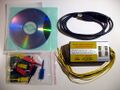
Package

Paper
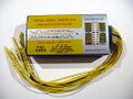
Device, top
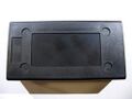
Device, bottom

Device, USB
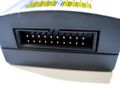
Device, connector
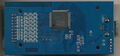
PCB, top
PCB, bottom
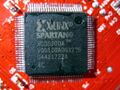
Xilinx XC3S200A
Altera EPM3032A
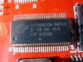
Cypress FX2
AT88SC0104 silkscreen
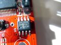
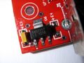
Microchip 24LC02B
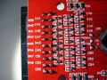
Input stage, 1
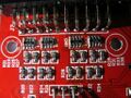
Input stage, 2
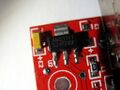
AMS1117-3.3
AMS1117-1.2


Revision 6.0:
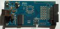
PCB, top
PCB, bottom
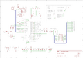
Schematic drawn from PCB


