Difference between revisions of "Hantek 6022BL"
Jump to navigation
Jump to search
(rephrase digital/analog selection under FX2 control) |
|||
| Line 15: | Line 15: | ||
* '''1A low-dropout voltage regulator (3.3V):''' [http://www.advanced-monolithic.com/products/voltreg.html#1117 Advanced Monolithic Systems AMS1117-3.3] [http://www.advanced-monolithic.com/pdf/ds1117.pdf datasheet]) | * '''1A low-dropout voltage regulator (3.3V):''' [http://www.advanced-monolithic.com/products/voltreg.html#1117 Advanced Monolithic Systems AMS1117-3.3] [http://www.advanced-monolithic.com/pdf/ds1117.pdf datasheet]) | ||
* '''2W, fixed input, isolated & unregulated dual/single output DC/DC converter''': [http://www.mornsun.cn/html/product/content/A_S-2WR2.html Mornsun A_S-2WR2 (A0505S-2WR2)] ([http://www.mornsun.cn/uploads/pdf/A_S-2WR2.pdf datasheet]) | * '''2W, fixed input, isolated & unregulated dual/single output DC/DC converter''': [http://www.mornsun.cn/html/product/content/A_S-2WR2.html Mornsun A_S-2WR2 (A0505S-2WR2)] ([http://www.mornsun.cn/uploads/pdf/A_S-2WR2.pdf datasheet]) | ||
* '''ADC''': ? | * '''ADC''': ? MXT2088, AD2988 compatible? (pinout matches, though the chip might differ) | ||
* '''?''': S1661SZ B212FG | * '''?''': S1661SZ B212FG | ||
* '''Crystal''': 24MHz | * '''Crystal''': 24MHz | ||
| Line 26: | Line 26: | ||
Discovered connections: | Discovered connections: | ||
* | * U2 is the Cypress FX2 controller, U4 is the '245 input buffer for digital probes, U8 is the ADC for two analog channels | ||
* | * FX2 PB and PD are connected to 16 lines of input data (shared among the digital buffer and the ADC output) | ||
* FX2 PA7 (pin 74) is directly connected to the digital buffer's OE signals (pins 25 and 48, low active, both 8bit groups share the signal) as well as DIR (pins 1 and 24) | |||
* | * FX2 PA7 is also connected to the ADC's S1 signal (pin 8, via two discrete inverters with R37, Q2, R13, Q1), S2 (pin 9) is tied to GND | ||
* | * according to the ADC datasheet (table 4), low/high signals on S1 and low on S2 result in either "standby mode" or "normal operation", respectively | ||
* with the digital buffer's OE signal being low active, low/high results in "active" and "tristate", respectively | |||
* this means: PA7 selects between digital (low) and analog (high) data paths, data is always at ports PB and PD, and either carries 16 digital channels, or two eight bit analog channels | |||
* the benefit of "variable DIR" in the digital buffer is questionable, since it shares the signal with OE and for high levels the output is high-Z anyway -- so the ADC output is _not_ routed to digital pins when PA7 is high, not tying DIR to a fixed level is pointless(?) | |||
== Photos == | == Photos == | ||
Revision as of 14:03, 26 December 2016
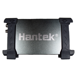
The Hantek 6022BL is a USB-based, 2-channel oscilloscope with an analog bandwidth of 20MS/s and 48MS/s sampling rate, and an 8-channel logic analyzer with 24MHz sampling rate.
See Hantek_6022BL/Info for more details (such as lsusb -v output) about the device.
Note: Currently only the logic analyzer part is supported, the oscilloscope part is work in progress.
Hardware
- USB: Cypress CY7C68013A-100AXC (FX2LP) (datasheet)
- 256-byte I²C EEPROM: 2x Microchip 24LC02BI (datasheet)
- 16-Bit bus transceiver with 3-state outputs: TI SN74LVC16245A (datasheet)
- 8-channel analog mux/demux: NXP 74HC4051D (datasheet)
- 1A low-dropout voltage regulator (3.3V): Advanced Monolithic Systems AMS1117-3.3 datasheet)
- 2W, fixed input, isolated & unregulated dual/single output DC/DC converter: Mornsun A_S-2WR2 (A0505S-2WR2) (datasheet)
- ADC: ? MXT2088, AD2988 compatible? (pinout matches, though the chip might differ)
- ?: S1661SZ B212FG
- Crystal: 24MHz
- Probes: 2x PP80B 1X/10X 80MHz bandwidth oscilloscope probes
- Attenuator: Hantek HT-201 20:1 attenuator (10MHz bandwidth, 1.053M input resistance)
The device has a "H/P" button. Depending on whether or not it's pressed it comes up with different USB VID/PIDs:
- Pressed: 04b4:602a Cypress Semiconductor Corp. (used for oscilloscope mode)
- Not pressed: 0925:3881 Lakeview Research Saleae Logic (Saleae Logic VID/PID, so fx2lafw works out of the box)
Discovered connections:
- U2 is the Cypress FX2 controller, U4 is the '245 input buffer for digital probes, U8 is the ADC for two analog channels
- FX2 PB and PD are connected to 16 lines of input data (shared among the digital buffer and the ADC output)
- FX2 PA7 (pin 74) is directly connected to the digital buffer's OE signals (pins 25 and 48, low active, both 8bit groups share the signal) as well as DIR (pins 1 and 24)
- FX2 PA7 is also connected to the ADC's S1 signal (pin 8, via two discrete inverters with R37, Q2, R13, Q1), S2 (pin 9) is tied to GND
- according to the ADC datasheet (table 4), low/high signals on S1 and low on S2 result in either "standby mode" or "normal operation", respectively
- with the digital buffer's OE signal being low active, low/high results in "active" and "tristate", respectively
- this means: PA7 selects between digital (low) and analog (high) data paths, data is always at ports PB and PD, and either carries 16 digital channels, or two eight bit analog channels
- the benefit of "variable DIR" in the digital buffer is questionable, since it shares the signal with OE and for high levels the output is high-Z anyway -- so the ADC output is _not_ routed to digital pins when PA7 is high, not tying DIR to a fixed level is pointless(?)
Photos
Protocol
When the "H/P" button is not pressed, the device can be used as 8-channel 24MHz logic analyzer via fx2lafw out of the box (using the fx2lafw protocol).


